SNAS515G July 2011 – December 2014 DAC161P997
PRODUCTION DATA.
- 1 Features
- 2 Application
- 3 Description
- 4 Revision History
- 5 Pin Configuration and Functions
- 6 Specifications
- 7 Detailed Description
- 8 Application and Implementation
- 9 Power Supply Recommendations
- 10Layout
- 11Device and Documentation Support
- 12Mechanical, Packaging, and Orderable Information
パッケージ・オプション
メカニカル・データ(パッケージ|ピン)
- RGH|16
サーマルパッド・メカニカル・データ
- RGH|16
発注情報
5 Pin Configuration and Functions
WQFN (RGH0016A)
16 pins
Top View
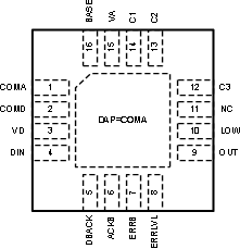
Pin Functions
| PIN | DESCRIPTION | ESD PROTECTION | |
|---|---|---|---|
| NAME | NO. | ||
| VA | 15 | Analog block positive supply rail |
 |
| COMA | 1 | Analog block negative supply rail (local COMMMON) |
 |
| COMD | 2 | Digital block negative supply rail (local COMMON) |
 |
| VD | 3 | Digital block positive supply rail |
 |
| DIN | 4 | SWIF input | |
| DBACK | 5 | SWIF input loop back | |
| ACKB | 6 | SWIF acknowledge output - open drain, active LOW | |
| ERRLVL | 8 | Sets the output current level at power-up | |
| LOW | 10 | Must be tied to COMA, COMD potential | |
| C1 | 14 | External capacitor | |
| C2 | 13 | External capacitor, HART Input | |
| C3 | 12 | External capacitor | |
| BASE | 16 | External NPN base drive | |
| N.C. | 11 | User must not connect to this pin | |
| ERRB | 7 | Error flag output open drain, active LOW |
 |
| OUT | 9 | Loop output current source |
 |
| DAP | - | Die Attach Pad. For best thermal conductivity and best noise immunity DAP should be soldered to the PCB pad which is connected directly to circuit common node (COMA, COMD) | - |