SNAS515G July 2011 – December 2014 DAC161P997
PRODUCTION DATA.
- 1 Features
- 2 Application
- 3 Description
- 4 Revision History
- 5 Pin Configuration and Functions
- 6 Specifications
- 7 Detailed Description
- 8 Application and Implementation
- 9 Power Supply Recommendations
- 10Layout
- 11Device and Documentation Support
- 12Mechanical, Packaging, and Orderable Information
パッケージ・オプション
メカニカル・データ(パッケージ|ピン)
- RGH|16
サーマルパッド・メカニカル・データ
- RGH|16
発注情報
6 Specifications
6.1 Absolute Maximum Ratings
over operating free-air temperature range (unless otherwise noted) (1)| MIN | MAX | UNIT | ||
|---|---|---|---|---|
| Supply relative to common (VA, VD to COMA, COMD) | −0.3 | 6 | V | |
| Voltage between any 2 pins(1) | 6 | V | ||
| Current IN or OUT of any pin - except OUT(1) | 5 | mA | ||
| Output current at OUT | 50 | mA | ||
| Junction Temperature | ||||
| Storage temperature range, Tstg | −65 | 150 | °C | |
(1) Stresses beyond those listed under Absolute Maximum Ratings may cause permanent damage to the device. These are stress ratings only, which do not imply functional operation of the device at these or any other conditions beyond those indicated under Recommended Operating Conditions. Exposure to absolute-maximum-rated conditions for extended periods may affect device reliability.
6.2 ESD Ratings
| VALUE | UNIT | |||
|---|---|---|---|---|
| V(ESD) | Electrostatic discharge | Human-body model (HBM), per ANSI/ESDA/JEDEC JS-001(1) | ±5500 | V |
| Charged-device model (CDM), per JEDEC specification JESD22-C101(2) | ±1250 | |||
(1) JEDEC document JEP155 states that 500-V HBM allows safe manufacturing with a standard ESD control process.
(2) JEDEC document JEP157 states that 250-V CDM allows safe manufacturing with a standard ESD control process.
6.3 Recommended Operating Conditions
| MIN | MAX | UNIT | |||
|---|---|---|---|---|---|
| Supply Voltage Range | 2.7 | 3.6 | V | ||
| (VA - VD) | 0 | 0 | V | ||
| (COMA - COMD) | 0 | 0 | V | ||
| BASE load to COMA | 0 | 15 | pF | ||
| OUT load to COMA | - | - | |||
| Operating Temperature (TA) | -40 | 105 | °C | ||
6.4 Thermal Information
| THERMAL METRIC(1) | WQFN (16-PINS) | UNIT | |
|---|---|---|---|
| RθJA | Junction-to-ambient thermal resistance | 35 | °C/W |
(1) For more information about traditional and new thermal metrics, see the IC Package Thermal Metrics application report, SPRA953.
6.5 Electrical Characteristics
Unless otherwise noted, these specifications apply for VA = VD = 2.7 V to 3.6 V, TA = 25°C, external bipolar transistor: 2N3904, RE = 22Ω, C1 = C2 = C3 = 2.2 nF.| PARAMETER | TEST CONDITIONS | MIN | TYP | MAX | UNIT | |
|---|---|---|---|---|---|---|
| POWER SUPPLY | ||||||
| VA, VD | Supply Voltage | VA = VD | 2.7 | 3.6 | V | |
| VA Supply Current | DACCODE=0x0200(2)
-40 to 105°C |
75 | µA | |||
| VD Supply Current | 115 | µA | ||||
| Total Supply Current | 190 | µA | ||||
| VPOR | Power On Reset supply rail potential threshold | 1.3 | 1.9 | V | ||
| DC ACCURACY | ||||||
| N | Resolution | 16 | Bits | |||
| INL | Integral Non-Linearity(6) | 0x2AAA < DACCODE < 0xD555 (4mA < ILOOP < 20 mA) -40 to 105°C |
–2.1 | 3.3 | µA | |
| DNL | Differential Non-Linearity | See(7)
-40 to 105°C |
–0.2 | 0.2 | ||
| TUE | Total Unadjusted Error | 0x2AAA < DACCODE < 0xD555 | –0.23% | 0.23% | FS | |
| OE | Offset Error | See(3)
-40 to 105°C |
−9.16 | 9.16 | µA | |
| Offset Error Temp. Coefficient | 138 | nA/°C | ||||
| GE | Gain Error | See(4)
-40 to 105°C |
−0.22% | 0.22% | FS | |
| Gain Error Temp. Coefficient | 5 | 29 | ppmFS/°C | |||
| 4 mA Loop Current Error | DACCODE = 0x2AAA -40 to 105°C |
−18 | 18 | µA | ||
| 20 mA Loop Current Error | DACCODE = 0xD555 -40 to 105°C |
−55 | 55 | |||
| IERRL | LOW ERROR Current | ERR_LOW = default -40 to 105°C |
3361 | 3375 | 3391 | |
| IERRH | HIGH ERROR Current | ERR_HIGH = default -40 to 105°C |
21702 | 21750 | 21817 | |
| LTD | Long Term Drift — mean shift of 12 mA output current after 1000 hrs at 150°C | 90 | ppmFS | |||
| LOOP CURRENT OUTPUT (OUT) | ||||||
| Output Current | Minimum tested at DACCODE = 0x01C2(5)
-40 to 105°C |
0.18 | 24 | mA | ||
| Output Impedance | 100 | MΩ | ||||
| COMA to OUT voltage drop | IOUT = 24 mA | 960 | mV | |||
| BASE OUTPUT | ||||||
| BASE short circuit output current | BASE forced to COMA potential | 10 | mA | |||
| DYNAMIC CHARACTERISTICS | ||||||
| Output Noise Density | 1 kHz | 20 | nA/√Hz | |||
| Integrated Output Noise | 1 Hz to 1 kHz band | 300 | nARMS | |||
| SWIF I/O CHARACTERISTICS | ||||||
| VIH | DIN | -40 to 105°C | 0.7* VD | V | ||
| VIL | DIN | -40 to 105°C | 0.3*VD | |||
| CDIN | DIN input capacitance | 10 | pF | |||
| VOH | DBACK | I = 3 mA -40 to 105°C |
2216 | mV | ||
| I = 5 mA -40 to 105°C |
1783 | |||||
| VOL | DBACK | I = 3 mA -40 to 105°C |
547 | |||
| I = 5 mA -40 to 105°C |
1260 | |||||
| TD | DIN to DBACK delay | 8 | ns | |||
| OPEN DRAIN OUTPUTS | ||||||
| VOL | ACKB | I = 3 mA -40 to 105°C |
550 | mV | ||
| I = 5 mA -40 to 105°C |
1370 | |||||
| VOL | ERRB | I = 300 µA -40 to 105°C |
66 | mV | ||
| I = 3 mA -40 to 105°C |
602 | |||||
| IOZ | ACKB | Leakage current when output device is off -40 to 105°C |
1 | µA | ||
| ERRB | Leakage current when output device is off -40 to 105°C |
1 | ||||
(1) When the input voltage (VIN) at any pin exceeds power supplies (VIN < COMA or VIN > VA), the current at that pin must not exceed 5 mA, and the voltage (VIN) at that pin relative to any other pin must not exceed 6.0V. See Pin Fuctions for additional details of input structures.
(2) At code 0x0200 the BASE current is minimal, i.e., device current contribution to power consumption is minimized. The SWIF link is inactive, i.e., after transmitting code 0x200 to the DAC161P997, there are no more transitions in the channel during the supply current measurement.
(3) Here offset is the y-intercept of the straight line defined by 4-mA and 20-mA points of the measured transfer characteristic.
(4) Here Gain Error is the difference in slope of the straight line defined by measured 4-mA and 20-mA points of transfer characteristic, and that of the ideal characteristic.
(5) This should be treated as the minimum LOOP current ensured specification.
(6) INL is measured using “best fit” method in the output current range of 4 mA to 20 mA.
(7) Specified by design.
6.6 Timing Requirements
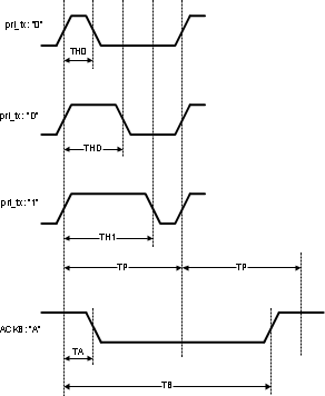
Figure 1. Single-Wire Interface (SWIF) Timing Diagram
6.7 Typical Characteristics
Unless otherwise noted, data presented here was collected under these conditions VA = VD = 3.3V, TA = 25°C, external bipolar transistor: 2N3904, RE = 22Ω, C1 = C2 = C3 = 2.2 nF.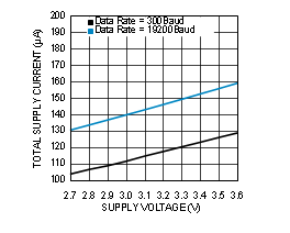 Figure 2. Supply Current vs Supply Voltage
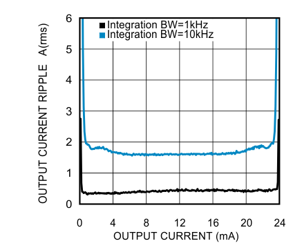 Figure 4. Integrated Noise vs ILOOP
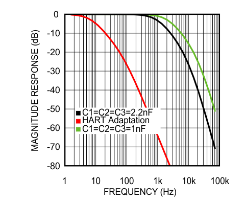 Figure 6. ΣΔ Modulator Filter Response
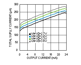 Figure 8. Supply Current vs ILOOP
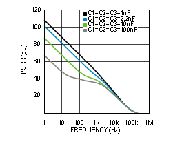 Figure 10. PSRR: ILOOP=4 mA
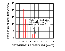 Figure 3. Gain Error TC Distribution
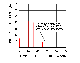 Figure 5. Offset Error TC Distribution
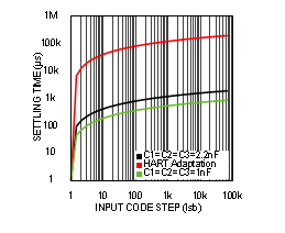 Figure 7. Settling Time vs Input Step Size
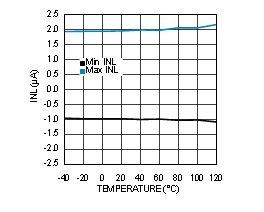 Figure 9. Output Linearity vs Temperature
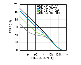 Figure 11. PSRR: ILOOP=20 mA