JAJSF31B November 2017 – June 2019 DLP3030-Q1
PRODUCTION DATA.
- 1 特長
- 2 アプリケーション
- 3 概要
- 4 改訂履歴
- 5 Pin Configuration and Functions
-
6 Specifications
- 6.1 Absolute Maximum Ratings
- 6.2 Storage Conditions
- 6.3 ESD Ratings
- 6.4 Recommended Operating Conditions
- 6.5 Thermal Information
- 6.6 Electrical Characteristics
- 6.7 Timing Requirements
- 6.8 Switching Characteristics
- 6.9 System Mounting Interface Loads
- 6.10 Physical Characteristics of the Micromirror Array
- 6.11 Optical Characteristics of the Micromirror Array
- 6.12 Window Characteristics
- 6.13 Chipset Component Usage Specification
- 7 Detailed Description
- 8 Application and Implementation
- 9 Power Supply Recommendations
- 10Layout
- 11デバイスおよびドキュメントのサポート
- 12メカニカル、パッケージ、および注文情報
7.3.6 Temperature Sensing Diode
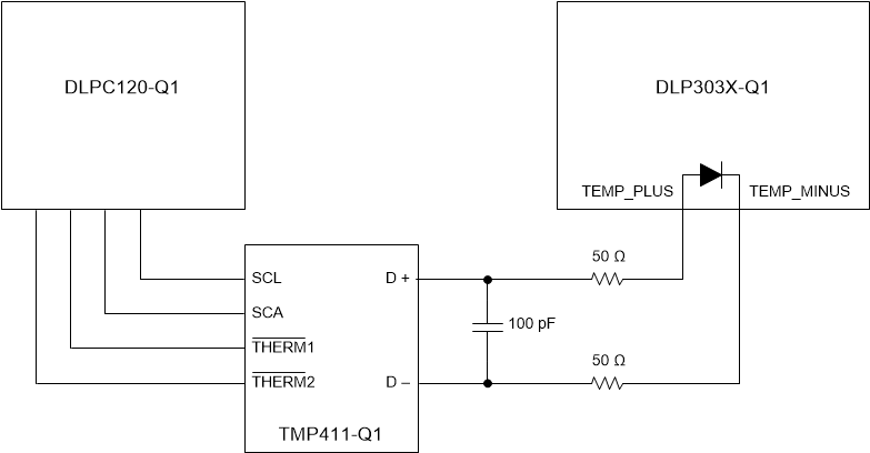
The DMD includes a temperature sensing diode designed to be used with the TMP411-Q1 temperature monitoring device. The DLPC120-Q1 monitors the DMD array temperature via the TMP411-Q1 and temperature sense diode. The DLPC120-Q1 operation of the DMD is based in part on the DMD array temperature, and therefore, this connection is essential to ensure reliable operation of the DMD.
Figure 9 shows the typical connection between the DLPC120-Q1, TMP411-Q1, and the DLP3030-Q1 DMD. The signals to the temperature sense diode are sensitive to system noise, therefore, care should be taken in the routing and implementation of this circuit. See the TMP411-Q1 Data Sheet for detailed PCB layout recommendations.
 Figure 9. Temperature Sense Diode Typical Circuit Configuration
 The DLPC120-Q1 automatically controls the DMD parking based on the temperature measured from the temperature sense diode; however, it is recommended that the host controller manage the parking via the proper methods described in the DLPC120-Q1 Programmer's Guide.