JAJSF31B November   2017  – June 2019 DLP3030-Q1

PRODUCTION DATA.  

  1. 特長
  2. アプリケーション
  3. 概要
    1.     Device Images
      1.      DLP DLP3030-Q1のブロック・システム図
  4. 改訂履歴
  5. Pin Configuration and Functions
    1.     Pin Configurations and Functions
  6. Specifications
    1. 6.1  Absolute Maximum Ratings
    2. 6.2  Storage Conditions
    3. 6.3  ESD Ratings
    4. 6.4  Recommended Operating Conditions
    5. 6.5  Thermal Information
    6. 6.6  Electrical Characteristics
    7. 6.7  Timing Requirements
    8. 6.8  Switching Characteristics
    9. 6.9  System Mounting Interface Loads
    10. 6.10 Physical Characteristics of the Micromirror Array
    11. 6.11 Optical Characteristics of the Micromirror Array
    12. 6.12 Window Characteristics
    13. 6.13 Chipset Component Usage Specification
  7. Detailed Description
    1. 7.1 Overview
    2. 7.2 Functional Block Diagram
    3. 7.3 Feature Description
      1. 7.3.1 Micromirror Array
      2. 7.3.2 Double Data Rate (DDR) Interface
      3. 7.3.3 Micromirror Switching Control
      4. 7.3.4 DMD Voltage Supplies
      5. 7.3.5 Logic Reset
      6. 7.3.6 Temperature Sensing Diode
        1. 7.3.6.1 Temperature Sense Diode Theory
      7. 7.3.7 Active Array Temperature
      8. 7.3.8 DMD JTAG Interface
    4. 7.4 Optical Performance
      1. 7.4.1 Numerical Aperture and Stray Light Control
      2. 7.4.2 Pupil Match
      3. 7.4.3 Illumination Overfill and Alignment
    5. 7.5 DMD Image Quality Specification
    6. 7.6 Definition of Micromirror Landed-On/Landed-Off Duty Cycle
  8. Application and Implementation
    1. 8.1 Application Information
    2. 8.2 Typical Application
      1. 8.2.1 HUD Reference Design and LED Controller Reference Design
    3. 8.3 Application Mission Profile Consideration
  9. Power Supply Recommendations
    1. 9.1 Power Supply Sequencing Requirements
      1. 9.1.1 Power Up and Power Down
  10. 10Layout
    1. 10.1 Layout Guidelines
    2. 10.2 Temperature Diode Pins
    3. 10.3 Layout Example
  11. 11デバイスおよびドキュメントのサポート
    1. 11.1 デバイス・サポート
      1. 11.1.1 デバイスの項目表記
      2. 11.1.2 デバイスのマーキング
    2. 11.2 ドキュメントのサポート
      1. 11.2.1 関連資料
    3. 11.3 ドキュメントの更新通知を受け取る方法
    4. 11.4 コミュニティ・リソース
    5. 11.5 商標
    6. 11.6 静電気放電に関する注意事項
    7. 11.7 デバイスの取り扱い
    8. 11.8 Glossary
  12. 12メカニカル、パッケージ、および注文情報

パッケージ・オプション

メカニカル・データ(パッケージ|ピン)
サーマルパッド・メカニカル・データ
発注情報

Temperature Sense Diode Theory

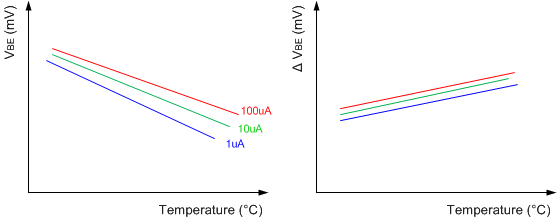
A temperature sensing diode is based on the fundamental current and temperature characteristics of a transistor. The diode is formed by connecting the transistor base to the collector. Two different known currents flow through the diode and the resulting diode voltage is measured in each case. The difference in their base-emitter voltages is proportional to the absolute temperature of the transistor.

Refer to the TMP411-Q1 Data Sheet for detailed information about temperature diode theory and measurement. Figure 10 and Figure 11 illustrate the relationship between the current and voltage through the diode.
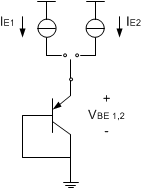
DLP3030-Q1 temp_sens_diode_theory.gifFigure 10. Temperature Measurement Theory
DLP3030-Q1 temp_sense_diode_theory_vbe.gifFigure 11. Example of Delta VBE vs Temperature