DLPS031C December 2013 – August 2015 DLPC6401
PRODUCTION DATA.
- 1 Features
- 2 Applications
- 3 Description
- 4 Revision History
- 5 Pin Configuration and Functions
-
6 Specifications
- 6.1 Absolute Maximum Ratings
- 6.2 ESD Ratings
- 6.3 Recommended Operating Conditions
- 6.4 Thermal Information
- 6.5 Electrical Characteristics
- 6.6 Electrical Characteristics (Normal Mode)
- 6.7 System Oscillators Timing Requirements
- 6.8 Test and Reset Timing Requirements
- 6.9 JTAG Interface: I/O Boundary Scan Application Timing Requirements
- 6.10 Port 1 Input Pixel Interface Timing Requirements
- 6.11 Port 2 Input Pixel Interface (FPD-Link Compatible LVDS Input) Timing Requirements
- 6.12 Synchronous Serial Port (SSP) Interface Timing Requirements
- 6.13 Programmable Output Clocks Switching Characteristics
- 6.14 Synchronous Serial Port (SSP) Interface Switching Characteristics
- 6.15 JTAG Interface: I/O Boundary Scan Application Switching Characteristics
- 7 Detailed Description
- 8 Application and Implementation
- 9 Power Supply Recommendations
- 10Layout
- 11Device and Documentation Support
- 12Mechanical, Packaging, and Orderable Information
10.1.1 PCB Layout Guidelines for Internal ASIC Power
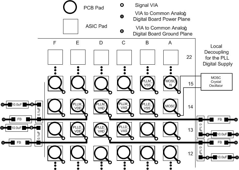
TI recommends the following guidelines to achieve desired ASIC performance relative to internal PLLs:
- The DLPC6401 device contains two PLLs (PLLM and PLLD), each of which has a dedicated 1.2-V digital and 1.8-V analog supply. These 1.2-V PLL pins should be individually isolated from the main 1.2-V system supply through a ferrite bead. The impedance of the ferrite bead should be much greater than that of the capacitor at frequencies where noise is expected. Specifically the impedance of the ferrite bead must be less than 0.5 Ω in the frequency range of 100 to 300 kHz and greater than 10 Ω in the frequency range >100 MHz.
- As a minimum, 1.8-V analog PLL power and ground pins should be isolated using an LC-filter with a ferrite serving as the inductor and a 0.1-µF capacitor on the ASIC side of the ferrite. TI recommends that this 1.8-V PLL power be supplied from a dedicated linear regulator and each PLL should be individually isolated from the regulator. The same ferrite recommendations described for the 1.2-V digital PLL supply apply to the 1.8-V analog PLL supplies.
- When designing the overall supply filter network, take care to ensure no resonance occurs. Particularly take care around the 1- to 2-mHz band, as this coincides with the PLL natural loop frequency.
 Figure 18. PLL Filter Layout
High-frequency decoupling is required for both 1.2-V and 1.8-V PLL supplies and should be provided as close as possible to each of the PLL supply package pins. TI recommends placing decoupling capacitors under the package on the opposite side of the board. Use high-quality, low-ESR, monolithic, surface mount capacitors. Typically 0.1 µF for each PLL supply should be sufficient. The length of a connecting trace increases the parasitic inductance of the mounting, and thus, where possible, there should be no trace, allowing the via to butt up against the land itself. Additionally, the connecting trace should be made as wide as possible. Further improvement can be made by placing vias to the side of the capacitor lands or doubling the number of vias.
The location of bulk decoupling depends on the system design. Typically, a good ceramic capacitor in the 10-µF range is adequate.