JAJSK47D August 2020 – December 2023 DP83TD510E
PRODUCTION DATA
- 1
- 1 特長
- 2 アプリケーション
- 3 概要
- 4 Pin Configuration and Functions
- 5 Specifications
-
6 Detailed Description
- 6.1 Overview
- 6.2 Functional Block Diagram
- 6.3
Feature Description
- 6.3.1 Auto-Negotiation (Speed Selection)
- 6.3.2 Repeater Mode
- 6.3.3 Media Converter
- 6.3.4 Clock Output
- 6.3.5 Media Independent Interface (MII)
- 6.3.6 Reduced Media Independent Interface (RMII)
- 6.3.7 RMII Low Power 5-MHz Mode
- 6.3.8 RGMII Interface
- 6.3.9 Serial Management Interface
- 6.3.10 Extended Register Space Access
- 6.3.11 Loopback Modes
- 6.3.12 BIST Configurations
- 6.3.13 Cable Diagnostics
- 6.4 Device Functional Modes
- 6.5 Programming
- 6.6 MMD Register Address Map
- 6.7 DP83TD510E Registers
- 7 Application and Implementation
- 8 Device and Documentation Support
- 9 Revision History
- 10Mechanical, Packaging, and Orderable Information
パッケージ・オプション
メカニカル・データ(パッケージ|ピン)
- RHB|32
サーマルパッド・メカニカル・データ
- RHB|32
発注情報
7.4.1.1 Signal Traces
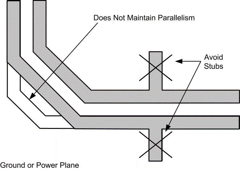
PCB traces are lossy and long traces can degrade signal quality. Keep traces as short as possible. Unless mentioned otherwise, all signal traces must be 50-Ω single-ended impedance. Differential traces must 100-Ω differential. Take care to ensure impedance is controlled throughout. Impedance discontinuities cause reflections leading to emissions and signal integrity issues. Stubs should be avoided on all signal traces, especially differential signal pairs.
 Figure 7-7 Differential Signal Traces
Within the differential pairs, trace lengths should be run parallel to each other and matched in length. Matched lengths minimize delay differences, avoiding an increase in common mode noise and emissions. Length matching is also important for MAC interface connections. All RMII transmit signal traces should be length matched to each other and all RMII receive signal traces should be length matched to each other.
Ideally, there should be no crossover or vias on signal path traces. Vias present impedance discontinuities and should be minimized when possible. Route trace pairs on the same layer. Signals on different layers should not cross each other without at least one return path plane between them. Differential pairs should always have a constant coupling distance between them. For convenience and efficiency, TI recommends routing critical signals first (that is, MDI differential pairs, reference clock, and MAC IF traces).