JAJSK47D August   2020  – December 2023 DP83TD510E

PRODUCTION DATA  

  1.   1
  2. 特長
  3. アプリケーション
  4. 概要
  5. Pin Configuration and Functions
    1.     Pin Functions
  6. Specifications
    1. 5.1 Absolute Maximum Ratings
    2. 5.2 ESD Ratings
    3. 5.3 Recommended Operating Conditions
    4. 5.4 Thermal Information
    5. 5.5 Electrical Characteristics
    6. 5.6 Timing Requirements
    7. 5.7 Timing Diagrams
  7. Detailed Description
    1. 6.1 Overview
    2. 6.2 Functional Block Diagram
    3. 6.3 Feature Description
      1. 6.3.1  Auto-Negotiation (Speed Selection)
      2. 6.3.2  Repeater Mode
      3. 6.3.3  Media Converter
      4. 6.3.4  Clock Output
      5. 6.3.5  Media Independent Interface (MII)
      6. 6.3.6  Reduced Media Independent Interface (RMII)
      7. 6.3.7  RMII Low Power 5-MHz Mode
      8. 6.3.8  RGMII Interface
      9. 6.3.9  Serial Management Interface
      10. 6.3.10 Extended Register Space Access
        1. 6.3.10.1 Read (No Post Increment) Operation
        2. 6.3.10.2 Read (Post Increment) Operation
        3. 6.3.10.3 Write (No Post Increment) Operation
        4. 6.3.10.4 Write (Post Increment) Operation
      11. 6.3.11 Loopback Modes
        1. 6.3.11.1 MII Loopback
        2. 6.3.11.2 PCS Loopback
        3. 6.3.11.3 Digital Loopback
        4. 6.3.11.4 Analog Loopback
        5. 6.3.11.5 Far-End (Reverse) Loopback
      12. 6.3.12 BIST Configurations
      13. 6.3.13 Cable Diagnostics
        1. 6.3.13.1 TDR
        2. 6.3.13.2 Fast Link Down Functionality
    4. 6.4 Device Functional Modes
      1. 6.4.1 Straps Configuration
        1. 6.4.1.1 Straps for PHY Address
    5. 6.5 Programming
    6. 6.6 MMD Register Address Map
    7. 6.7 DP83TD510E Registers
  8. Application and Implementation
    1. 7.1 Application Information
    2. 7.2 Typical Applications
      1. 7.2.1 Termination Circuit
        1. 7.2.1.1 Termination Circuit for Intrinsic Safe Applications
        2. 7.2.1.2 Components Range for Power Coupling/Decoupling
        3. 7.2.1.3 Termination Circuit for Non-Intrinsic Safe Applications
        4. 7.2.1.4 CMC Specifications
      2. 7.2.2 Design Requirements
        1. 7.2.2.1 Clock Requirements
          1. 7.2.2.1.1 Oscillator
          2. 7.2.2.1.2 Crystal
    3. 7.3 Power Supply Recommendations
    4. 7.4 Layout
      1. 7.4.1 Layout Guidelines
        1. 7.4.1.1 Signal Traces
        2. 7.4.1.2 Return Path
        3. 7.4.1.3 Metal Pour
        4. 7.4.1.4 PCB Layer Stacking
      2. 7.4.2 Layout Example
  9. Device and Documentation Support
    1. 8.1 Device Support
    2. 8.2 サポート・リソース
    3. 8.3 Trademarks
    4. 8.4 静電気放電に関する注意事項
    5. 8.5 用語集
  10. Revision History
  11. 10Mechanical, Packaging, and Orderable Information

パッケージ・オプション

メカニカル・データ(パッケージ|ピン)
サーマルパッド・メカニカル・データ
発注情報

Repeater Mode

The DP83TD510E provides an option to enable repeater mode functionality to extend the cable reach. Two DP83TD510E can be connected in back to back mode without any external configuration. A hardware strap is provided to configure the CRS_DV pin of RMII interface to RX_DV pin for back to back operation. Refer to RMII Repeater Mode for the RMII pin connection to enable repeater mode on the DP83TD510E, and Table 7-9 for the RX_DV strap setting. DP83TD510E RGMII MAC mode can also be used for Repeater Mode. With RGMII MAC, the MAC interface clock runs at 2.5 MHz and will dissipiate less power and offer improved signal integrity.
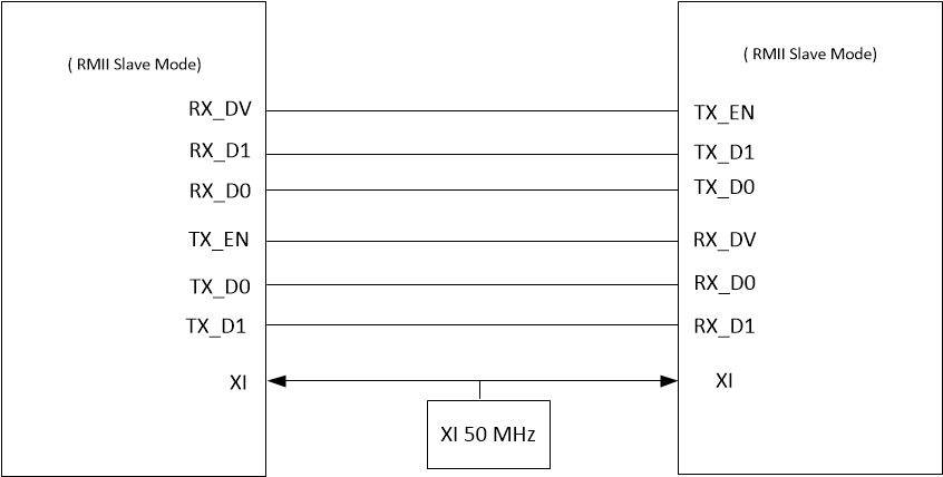
GUID-D7E67973-AB0F-4F82-985A-8B898AF46DE9-low.gif Figure 6-1 RMII Repeater Mode