SLVSCX2B August 2015 – February 2016 DRV8305
PRODUCTION DATA.
- 1 Features
- 2 Applications
- 3 Description
- 4 Revision History
- 5 Pin Configuration and Functions
- 6 Specifications
-
7 Detailed Description
- 7.1 Overview
- 7.2 Functional Block Diagram
- 7.3
Feature Description
- 7.3.1 Integrated Three-Phase Gate Driver
- 7.3.2 INHx/INLx: Gate Driver Input Modes
- 7.3.3 VCPH Charge Pump: High-Side Gate Supply
- 7.3.4 VCP_LSD LDO: Low-Side Gate Supply
- 7.3.5 GHx/GLx: Half-Bridge Gate Drivers
- 7.3.6 DVDD and AVDD: Internal Voltage Regulators
- 7.3.7 VREG: Voltage Regulator Output
- 7.3.8 Protection Features
- 7.3.9 Undervoltage Warning (UVFL), Undervoltage Lockout (UVLO), and Overvoltage (OV) Protection
- 7.4 Device Functional Modes
- 7.5 Programming
- 7.6
Register Maps
- 7.6.1 Status Registers
- 7.6.2
Control Registers
- 7.6.2.1 HS Gate Drive Control (Address = 0x5)
- 7.6.2.2 LS Gate Drive Control (Address = 0x6)
- 7.6.2.3 Gate Drive Control (Address = 0x7)
- 7.6.2.4 IC Operation (Address = 0x9)
- 7.6.2.5 Shunt Amplifier Control (Address = 0xA)
- 7.6.2.6 Voltage Regulator Control (Address = 0xB)
- 7.6.2.7 VDS Sense Control (Address = 0xC)
- 8 Application and Implementation
- 9 Power Supply Recommendations
- 10Layout
- 11Device and Documentation Support
- 12Mechanical, Packaging, and Orderable Information
パッケージ・オプション
メカニカル・データ(パッケージ|ピン)
- PHP|48
サーマルパッド・メカニカル・データ
- PHP|48
発注情報
10 Layout
10.1 Layout Guidelines
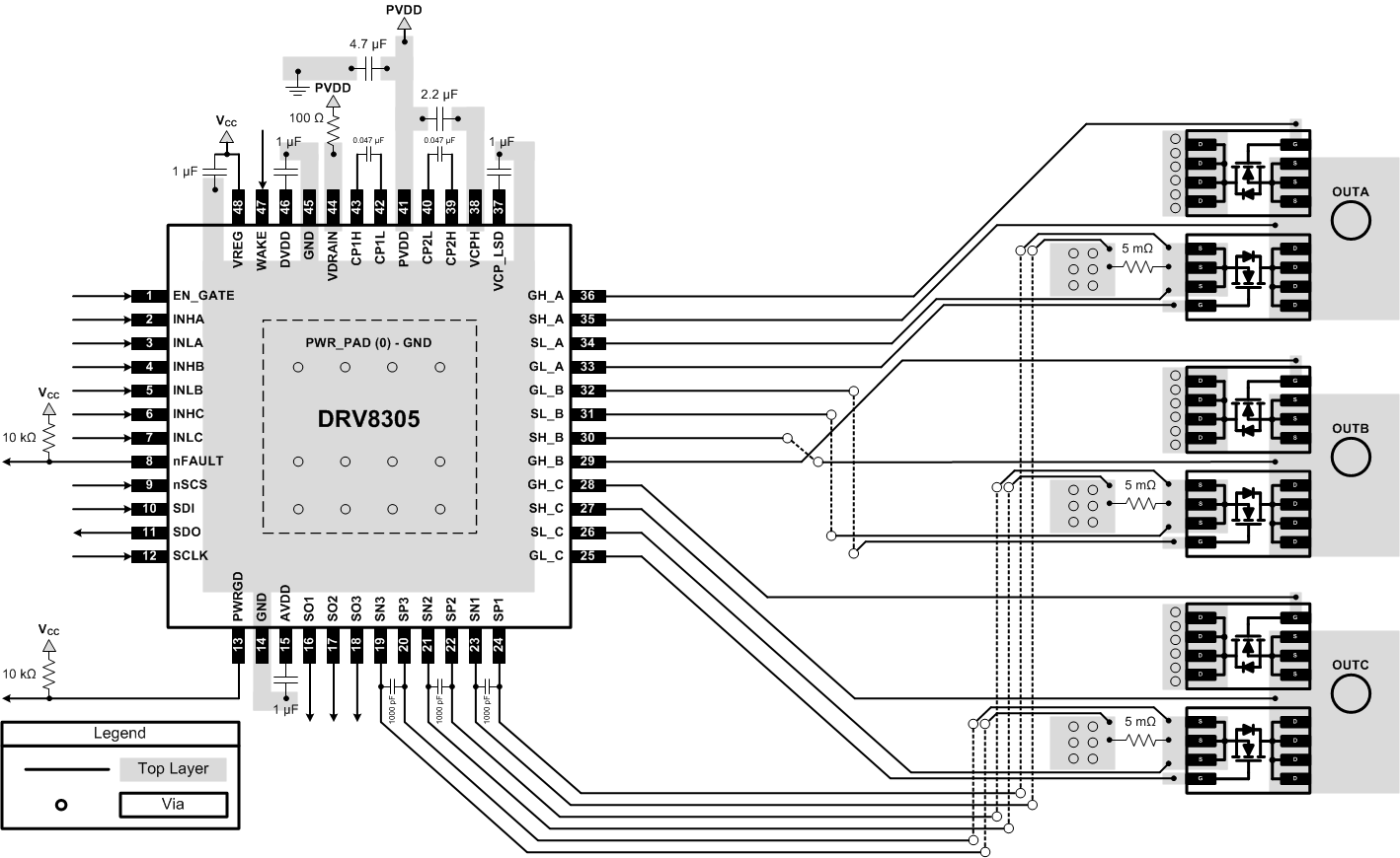
Use the following layout recommendations when designing a PCB for the DRV8305.
- The DVDD and AVDD 1-μF bypass capacitors should connect directly to the adjacent GND pin to minimize loop impedance for the bypass capacitor.
- The CP1 and CP2 0.047-μF flying capacitors should be placed directly next to the DRV8305 charge pump pins.
- The VCPH 2.2-μF and VCP_LSD 1-μF bypass capacitors should be placed close to their corresponding pins with a direct path back to the DRV8305 GND net.
- The PVDD 4.7-μF bypass capacitor should be placed as close as possible to the DRV8305 PVDD supply pin.
- Use the proper footprint as shown in the Mechanical, Packaging, and Orderable Information section.
- Minimize the loop length for the high-side and low-side gate drivers. The high-side loop is from the DRV8305 GH_X to the power MOSFET and returns through SH_X. The low-side loop is from the DRV8305 GL_X to the power MOSFET and returns through SL_X.
10.2 Layout Example
 Figure 24. Layout Recommendation