SLVSCX2B August   2015  – February 2016 DRV8305

PRODUCTION DATA.  

  1. Features
  2. Applications
  3. Description
  4. Revision History
  5. Pin Configuration and Functions
  6. Specifications
    1. 6.1 Absolute Maximum Ratings
    2. 6.2 ESD Ratings
    3. 6.3 Recommended Operating Conditions
    4. 6.4 Thermal Information
    5. 6.5 Electrical Characteristics
    6. 6.6 SPI Timing Requirements (Slave Mode Only)
    7. 6.7 Typical Characteristics
  7. Detailed Description
    1. 7.1 Overview
    2. 7.2 Functional Block Diagram
    3. 7.3 Feature Description
      1. 7.3.1 Integrated Three-Phase Gate Driver
      2. 7.3.2 INHx/INLx: Gate Driver Input Modes
      3. 7.3.3 VCPH Charge Pump: High-Side Gate Supply
      4. 7.3.4 VCP_LSD LDO: Low-Side Gate Supply
      5. 7.3.5 GHx/GLx: Half-Bridge Gate Drivers
        1. 7.3.5.1 IDRIVE: Gate Driver Output Current
        2. 7.3.5.2 TDRIVE: Gate Driver State Machine
        3. 7.3.5.3 CSAs: Current Shunt Amplifiers
      6. 7.3.6 DVDD and AVDD: Internal Voltage Regulators
      7. 7.3.7 VREG: Voltage Regulator Output
      8. 7.3.8 Protection Features
        1. 7.3.8.1 Fault and Warning Classification
        2. 7.3.8.2 MOSFET Shoot-Through Protection (TDRIVE)
        3. 7.3.8.3 MOSFET Overcurrent Protection (VDS_OCP)
          1. 7.3.8.3.1 MOSFET dV/dt Turn On Protection (TDRIVE)
          2. 7.3.8.3.2 MOSFET Gate Drive Protection (GDF)
        4. 7.3.8.4 Low-Side Source Monitors (SNS_OCP)
        5. 7.3.8.5 Fault and Warning Operating Modes
      9. 7.3.9 Undervoltage Warning (UVFL), Undervoltage Lockout (UVLO), and Overvoltage (OV) Protection
        1. 7.3.9.1 Overtemperature Warning (OTW) and Shutdown (OTSD) Protection
        2. 7.3.9.2 Reverse Supply Protection
        3. 7.3.9.3 MCU Watchdog
        4. 7.3.9.4 VREG Undervoltage (VREG_UV)
    4. 7.4 Device Functional Modes
      1. 7.4.1 Power Up Sequence
      2. 7.4.2 Standby State
      3. 7.4.3 Operating State
      4. 7.4.4 Sleep State
      5. 7.4.5 Limp Home or Fail Code Operation
    5. 7.5 Programming
      1. 7.5.1 SPI Communication
        1. 7.5.1.1 SPI
        2. 7.5.1.2 SPI Format
    6. 7.6 Register Maps
      1. 7.6.1 Status Registers
        1. 7.6.1.1 Warning and Watchdog Reset (Address = 0x1)
        2. 7.6.1.2 OV/VDS Faults (Address = 0x2)
        3. 7.6.1.3 IC Faults (Address = 0x3)
        4. 7.6.1.4 VGS Faults (Address = 0x4)
      2. 7.6.2 Control Registers
        1. 7.6.2.1 HS Gate Drive Control (Address = 0x5)
        2. 7.6.2.2 LS Gate Drive Control (Address = 0x6)
        3. 7.6.2.3 Gate Drive Control (Address = 0x7)
        4. 7.6.2.4 IC Operation (Address = 0x9)
        5. 7.6.2.5 Shunt Amplifier Control (Address = 0xA)
        6. 7.6.2.6 Voltage Regulator Control (Address = 0xB)
        7. 7.6.2.7 VDS Sense Control (Address = 0xC)
  8. Application and Implementation
    1. 8.1 Application Information
    2. 8.2 Typical Application
      1. 8.2.1 Design Requirements
      2. 8.2.2 Detailed Design Procedure
        1. 8.2.2.1 Gate Drive Average Current
        2. 8.2.2.2 MOSFET Slew Rates
        3. 8.2.2.3 Overcurrent Protection
        4. 8.2.2.4 Current Sense Amplifiers
      3. 8.2.3 Application Curves
  9. Power Supply Recommendations
    1. 9.1 Bulk Capacitance
  10. 10Layout
    1. 10.1 Layout Guidelines
    2. 10.2 Layout Example
  11. 11Device and Documentation Support
    1. 11.1 Documentation Support
    2. 11.2 Community Resources
    3. 11.3 Trademarks
    4. 11.4 Electrostatic Discharge Caution
    5. 11.5 Glossary
  12. 12Mechanical, Packaging, and Orderable Information

パッケージ・オプション

メカニカル・データ(パッケージ|ピン)
サーマルパッド・メカニカル・データ
発注情報

5 Pin Configuration and Functions

PHP Package
48-Pin HTQFP
Top View
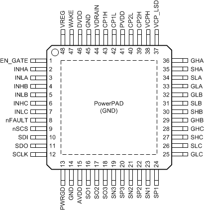
DRV8305 po_lvscx2.gif

Pin Functions

PIN TYPE DESCRIPTION
NAME NO.
EN_GATE 1 I Enable gate Enables the gate driver and current shunt amplifiers; internal pulldown
INHA 2 I Bridge PWM input PWM input signal for bridge A high side
INLA 3 I Bridge PWM input PWM input signal for bridge A low side
INHB 4 I Bridge PWM input PWM input signal for bridge B high side
INLB 5 I Bridge PWM input PWM input signal for bridge B low side
INHC 6 I Bridge PWM input PWM input signal for bridge C high side
INLC 7 I Bridge PWM input PWM input signal for bridge C low side
nFAULT 8 OD Fault indicator When low indicates a fault has occurred; open drain; external pullup to MCU power supply needed (1 kΩ to 10 kΩ)
nSCS 9 I SPI chip select Select/enable for SPI; active low
SDI 10 I SPI input SPI input signal
SDO 11 O SPI output SPI output signal
SCLK 12 I SPI clock SPI clock signal
PWRGD 13 OD Power good VREG and MCU watchdog fault indication; open drain; external pullup to MCU power supply needed (1 kΩ to 10 kΩ)
GND 14 P Device ground Must be connected to ground
45
AVDD 15 P Analog regulator 5-V internal analog supply regulator; bypass to GND with a 6.3-V, 1-µF ceramic capacitor
SO1 16 O Current amplifier output Output of current sense amplifier 1
SO2 17 O Current amplifier output Output of current sense amplifier 2
SO3 18 O Current amplifier output Output of current sense amplifier 3
SN3 19 I Current amplifier negative input Negative input of current sense amplifier 3
SP3 20 I Current amplifier positive input Positive input of current sense amplifier 3
SN2 21 I Current amplifier negative input Negative input of current sense amplifier 2
SP2 22 I Current amplifier positive input Positive input of current sense amplifier 2
SN1 23 I Current amplifier negative input Negative input of current sense amplifier 1
SP1 24 I Current amplifier positive input Positive input of current sense amplifier 1
GLC 25 O Low-side gate driver Low-side gate driver output for half-bridge C
SLC 26 I Low-side source connection Low-side source connection for half-bridge C
SHC 27 I High-side source connection High-side source connection for half-bridge C
GHC 28 O High-side gate driver High-side gate driver output for half-bridge C
GHB 29 O High-side gate driver High-side gate driver output for half-bridge B
SHB 30 I High-side source connection High-side source connection for half-bridge B
SLB 31 I Low-side source connection Low-side source connection for half-bridge B
GLB 32 O Low-side gate driver Low side gate driver output for half-bridge B
GLA 33 O Low-side gate driver Low-side gate driver output for half-bridge A
SLA 34 I Low-side source connection Low-side source connection for half-bridge A
SHA 35 I High-side source connection High-side source connection for half-bridge A
GHA 36 O High-side gate driver High-side gate driver output for half-bridge A
VCP_LSD 37 P Low-side gate driver regulator Internal voltage regulator for low-side gate driver; connect 1-µF capacitor to GND
VCPH 38 P High-side gate driver regulator Internal charge pump for high-side gate driver; connect 2.2-µF capacitor to PVDD
CP2H 39 P Charge pump flying capacitor Flying capacitor for charge pump; connect 0.047-µF capacitor between CP2H and CP2L
CP2L 40 P
PVDD 41 P Power supply Device power supply; minimum 4.7-µF ceramic capacitor to GND
CP1L 42 P Charge pump flying capacitor Flying capacitor for charge pump; connect 0.047-µF capacitor between CP1H and CP1L
CP1H 43 P
VDRAIN 44 P High-side drain High-side MOSFET drain connection; common for all three half bridges
DVDD 46 P Digital regulator 3.3-V internal digital-supply regulator; bypass to GND with a 6.3-V, 1-µF ceramic capacitor
WAKE 47 I Wake up from sleep control pin High voltage tolerant input pin to wake-up device from SLEEP; pin cannot be used to disable LDO; driver needs to be enabled and disabled separately
VREG 48 P VREG/VREF Dual purpose pin based on part number; also supplies internal amplifier reference voltage and SDO pullup.
VREG: 3.3-V or 5-V, 50-mA LDO; connect 1-µF to GND
VREF: Reference voltage; LDO disabled
PowerPAD (GND) P Device ground Must be connected to ground

External Components

COMPONENT PIN 1 PIN 2 RECOMMENDED
CPVDD PVDD GND 4.7-µF ceramic capacitor rated for PVDD
CAVDD AVDD GND 1-µF ceramic capacitor rated for 6.3 V
CDVDD DVDD GND 1-µF ceramic capacitor rated for 6.3 V
CVCPH VCPH PVDD 2.2-µF ceramic capacitor rated for 16 V
CVCP_LSD VCP_LSD GND 1-µF ceramic capacitor rated for 16 V
CCP1 CP1H CP1L 0.047-µF ceramic capacitor rated for PVDD
CCP2 CP2H CP2L 0.047-µF ceramic capacitor rated for PVDD × 2
CVREG VREG GND 1-µF ceramic capacitor rated for 6.3 V
RVDRAIN VDRAIN PVDD 100-Ω series resistor between VDRAIN and HS MOSFET DRAIN
RnFAULT nFAULT VCC (1) 1-10 kΩ pulled up the MCU power supply
RPWRGD PWRGD VCC (1) 1-10 kΩ pulled up the MCU power supply
(1) VCC is not a pin on the DRV8305, but a VCC supply voltage pullup is required for open-drain output nFAULT.