JAJSM96 may   2023 DRV8849

PRODUCTION DATA  

  1.   1
  2. 特長
  3. アプリケーション
  4. 概要
  5. Revision History
  6. Device Comparison
  7. Pin Configuration and Functions
  8. Specifications
    1. 7.1 Absolute Maximum Ratings
    2. 7.2 ESD Ratings
    3. 7.3 Recommended Operating Conditions
    4. 7.4 Thermal Information
    5. 7.5 Electrical Characteristics
    6. 7.6 Indexer Timing Requirements
    7. 7.7 Typical Operating Characteristics
  9. Detailed Description
    1. 8.1 Overview
    2. 8.2 Functional Block Diagram
    3. 8.3 Feature Description
      1. 8.3.1 Stepper Motor Driver Current Ratings
        1. 8.3.1.1 Peak Current Rating
        2. 8.3.1.2 RMS Current Rating
        3. 8.3.1.3 Full-Scale Current Rating
      2. 8.3.2 Microstepping Indexer
      3. 8.3.3 Controlling VREF with an MCU DAC
      4. 8.3.4 Current Regulation and Decay Modes
        1. 8.3.4.1 Smart tune Ripple Control
        2. 8.3.4.2 Smart tune Dynamic Decay
        3. 8.3.4.3 Blanking time
      5. 8.3.5 Charge Pump
      6. 8.3.6 Logic Level, tri-level and quad-level Pin Diagrams
      7. 8.3.7 nFAULT Pins
      8. 8.3.8 Protection Circuits
        1. 8.3.8.1 VM Undervoltage Lockout (UVLO)
        2. 8.3.8.2 VCP Undervoltage Lockout (CPUV)
        3. 8.3.8.3 Overcurrent Protection (OCP)
          1. 8.3.8.3.1 Latched Shutdown
          2. 8.3.8.3.2 Automatic Retry
        4. 8.3.8.4 Thermal Shutdown (OTSD)
          1. 8.3.8.4.1 Latched Shutdown
          2. 8.3.8.4.2 Automatic Retry
        5. 8.3.8.5 Fault Condition Summary
    4. 8.4 Device Functional Modes
      1. 8.4.1 Sleep Mode (nSLEEP = 0)
      2. 8.4.2 Disable Mode (nSLEEP = 1, ENABLE = 0)
      3. 8.4.3 Operating Mode (nSLEEP = 1, ENABLE = Hi-Z/1)
      4. 8.4.4 nSLEEP Reset Pulse
      5. 8.4.5 Functional Modes Summary
  10. Application and Implementation
    1. 9.1 Application Information
    2. 9.2 Typical Application
      1. 9.2.1 Design Requirements
      2. 9.2.2 Detailed Design Procedure
        1. 9.2.2.1 Stepper Motor Speed
        2. 9.2.2.2 Current Regulation
        3. 9.2.2.3 Decay Modes
        4. 9.2.2.4 Application Curves
  11. 10Layout
    1. 10.1 Layout Guidelines
    2. 10.2 Bulk Capacitance
  12. 11デバイスおよびドキュメントのサポート
    1. 11.1 関連資料
  13. 12Mechanical, Packaging, and Orderable Information

パッケージ・オプション

メカニカル・データ(パッケージ|ピン)
サーマルパッド・メカニカル・データ
発注情報

Stepper Motor Speed

The first step in configuring the DRV8849 requires the desired motor speed and microstepping level. If the target application requires a constant speed, then a square wave with frequency ƒstep must be applied to the corresponding STEP pin. If the target motor speed is too high, the motor does not spin. Make sure that the motor can support the target speed. Use Equation 1 to calculate ƒstep for a desired motor speed (v), microstepping level (nm), and motor full step angle (θstep)

Equation 1. GUID-FF5F0738-FBD3-4167-A8F6-484E813A45E4-low.gif

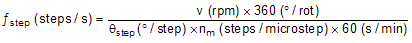
The value of θstep can be found in the stepper motor data sheet, or written on the motor. For example, the motors in this application are required to rotate at 1.8°/step for a target of 46.8 rpm at 1/32 microstep mode (for Motor 1); and for a target of 23.4 rpm at 1/256 microstep mode (for Motor 2). Using Equation 1, ƒstep can be calculated as 5 kHz for Motor 1 and 20 kHz for Motor 2.

The microstepping level is set by the MODE0x and MODE1x pins and can be any of the settings listed in Table 8-2. Higher microstepping results in a smoother motor motion and less audible noise, but requires a higher ƒstep to achieve the same motor speed.