JAJSRJ2A September 2000 – January 2024 INA114
PRODUCTION DATA
- 1
- 1 特長
- 2 アプリケーション
- 3 概要
- 4 Pin Configuration and Functions
- 5 Specifications
- 6 Application and Implementation
- 7 Typical Applications
- 8 Device and Documentation Support
- 9 Revision History
- 10Mechanical, Packaging, and Orderable Information
パッケージ・オプション
デバイスごとのパッケージ図は、PDF版データシートをご参照ください。
メカニカル・データ(パッケージ|ピン)
- P|8
- DW|16
サーマルパッド・メカニカル・データ
発注情報
6.1.7 Output Voltage Sense (SOIC-16 Package Only)
The surface-mount version of the INA114 has a separate output sense feedback connection (pin 12). Pin 12 must be connected to the output terminal (pin 11) for proper operation. (This connection is made internally on the DIP version of the INA114.)
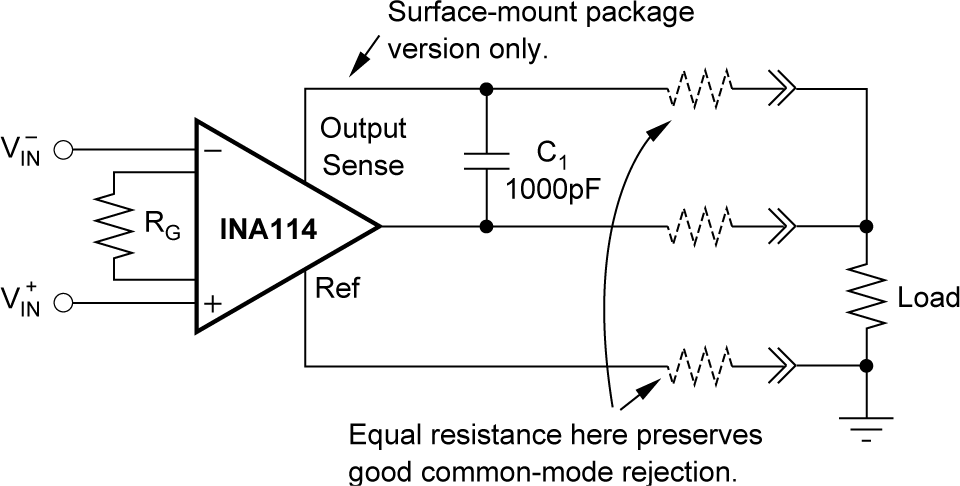
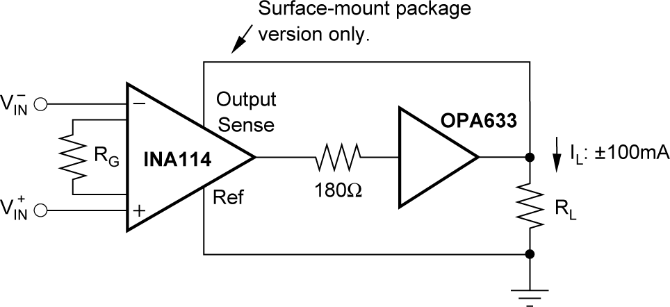
The output sense connection can be used to sense the output voltage directly at the load for best accuracy. Figure 6-5 shows how to drive a load through series interconnection resistance. Remotely located feedback paths can cause instability. This instability can be generally be eliminated with a high-frequency feedback path through C1. Drive heavy loads or long lines by connecting a buffer inside the feedback path (see Figure 6-6).
 Figure 6-5 Remote Load and Ground
Sensing
 Figure 6-6 Buffered Output for Heavy
Loads