JAJSDQ8D February   2013  – July 2022 INA231

PRODUCTION DATA  

  1. 特長
  2. アプリケーション
  3. 概要
  4. Revision History
  5. Device Comparison
  6. Pin Configuration and Functions
  7. Specifications
    1. 7.1 Absolute Maximum Ratings
    2. 7.2 ESD Ratings
    3. 7.3 Recommended Operating Conditions
    4. 7.4 Thermal Information
    5. 7.5 Electrical Characteristics
    6. 7.6 Timing Requirements: I2C Bus
    7. 7.7 Typical Characteristics
  8. Detailed Description
    1. 8.1 Overview
    2. 8.2 Functional Block Diagram
    3. 8.3 Feature Description
      1. 8.3.1 Basic Analog-to-Digital Converter (ADC) Functions
        1. 8.3.1.1 Power Calculation
        2. 8.3.1.2 ALERT Pin
    4. 8.4 Device Functional Modes
      1. 8.4.1 Averaging and Conversion Time Considerations
    5. 8.5 Programming
      1. 8.5.1 Configure, Measure, and Calculate Example
      2. 8.5.2 Programming the Power Measurement Engine
        1. 8.5.2.1 Calibration Register and Scaling
      3. 8.5.3 Simple Current Shunt Monitor Usage (No Programming Necessary)
      4. 8.5.4 Default INA231 Settings
      5. 8.5.5 Writing to and Reading from the INA231
        1. 8.5.5.1 Bus Overview
          1. 8.5.5.1.1 Serial Bus Address
          2. 8.5.5.1.2 Serial Interface
        2. 8.5.5.2 High-Speed I2C Mode
      6. 8.5.6 SMBus Alert Response
    6. 8.6 Register Maps
      1. 8.6.1 Configuration Register (00h, Read/Write)
        1. 8.6.1.1 AVG Bit Settings [11:9]
        2. 8.6.1.2 VBUS CT Bit Settings [8:6]
        3. 8.6.1.3 VSH CT Bit Settings [5:3]
        4. 8.6.1.4 Mode Settings [2:0]
      2. 8.6.2 Shunt Voltage Register (01h, Read-Only)
      3. 8.6.3 Bus Voltage Register (02h, Read-Only)
      4. 8.6.4 Power Register (03h, Read-Only)
      5. 8.6.5 Current Register (04h, Read-Only)
      6. 8.6.6 Calibration Register (05h, Read/Write)
      7. 8.6.7 Mask/Enable Register (06h, Read/Write)
      8. 8.6.8 Alert Limit Register (07h, Read/Write)
  9. Application and Implementation
    1. 9.1 Application Information
      1. 9.1.1 Filtering and Input Considerations
    2. 9.2 Typical Applications
      1. 9.2.1 Design Requirements
      2. 9.2.2 Detailed Design Procedure
      3. 9.2.3 Application Curves
    3. 9.3 Power Supply Recommendations
    4. 9.4 Layout
      1. 9.4.1 Layout Guidelines
      2. 9.4.2 Layout Example
  10. 10Device and Documentation Support
    1. 10.1 Documentation Support
      1. 10.1.1 Related Documentation
    2. 10.2 Receiving Notification of Documentation Updates
    3. 10.3 サポート・リソース
    4. 10.4 Trademarks
    5. 10.5 Electrostatic Discharge Caution
    6. 10.6 Glossary
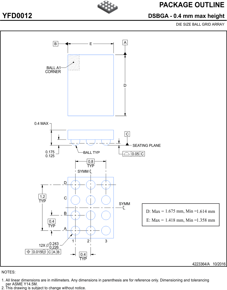
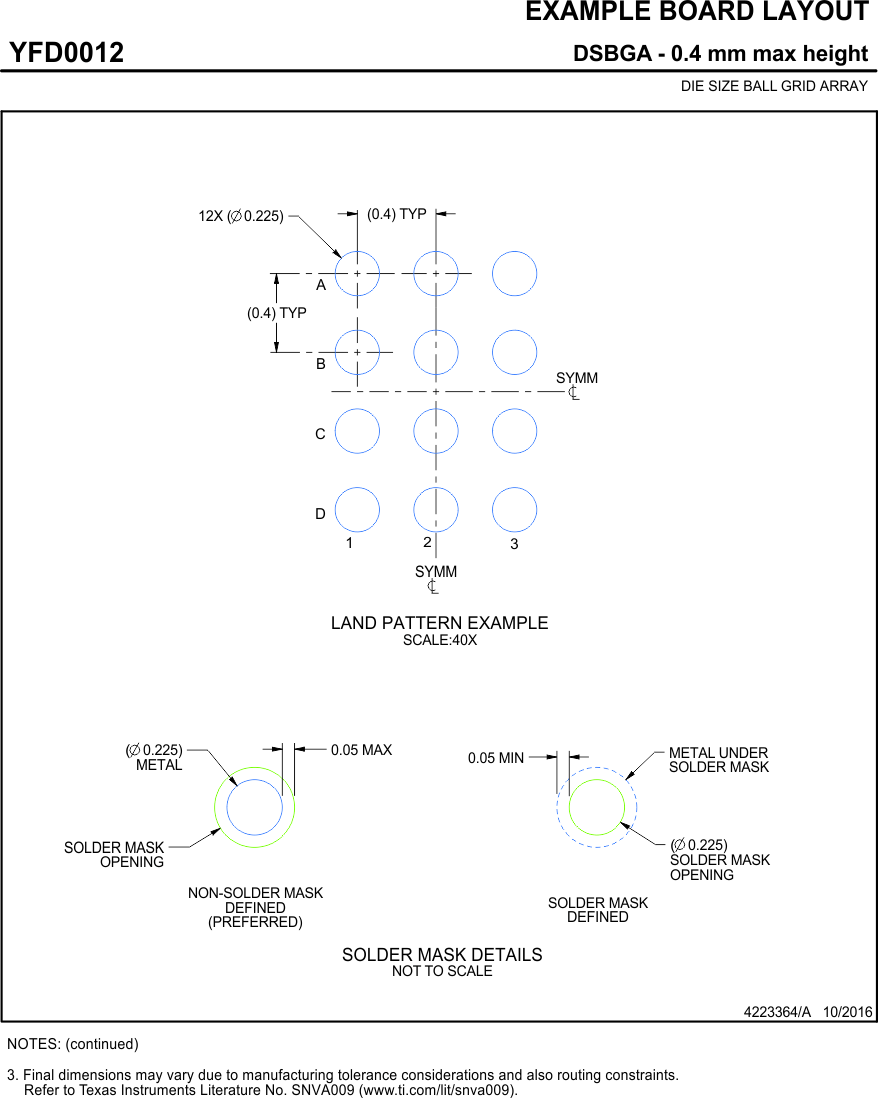
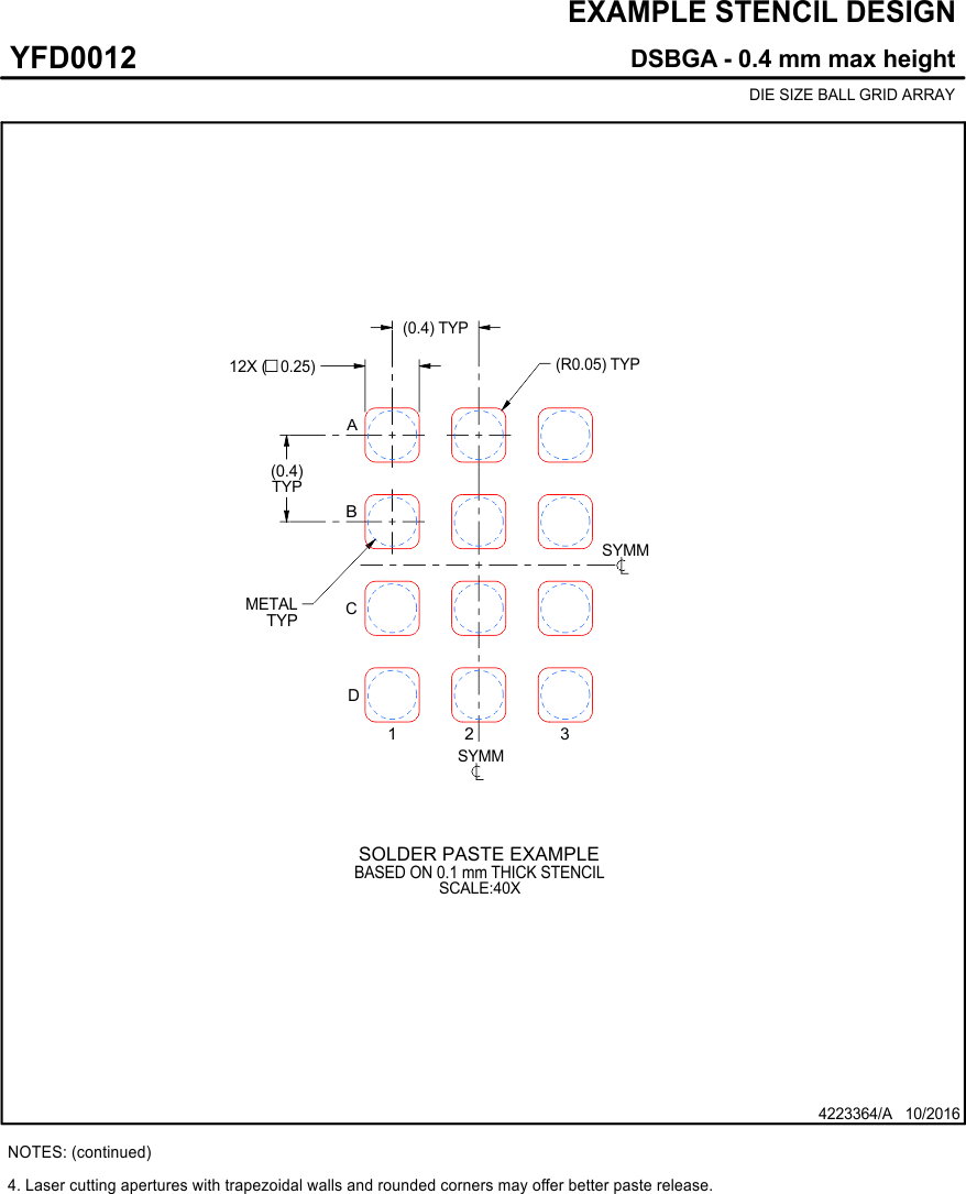
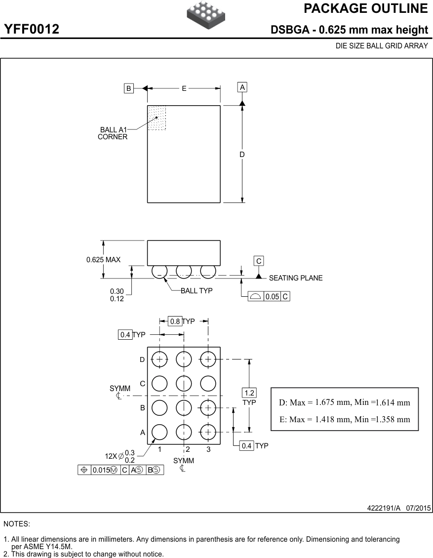
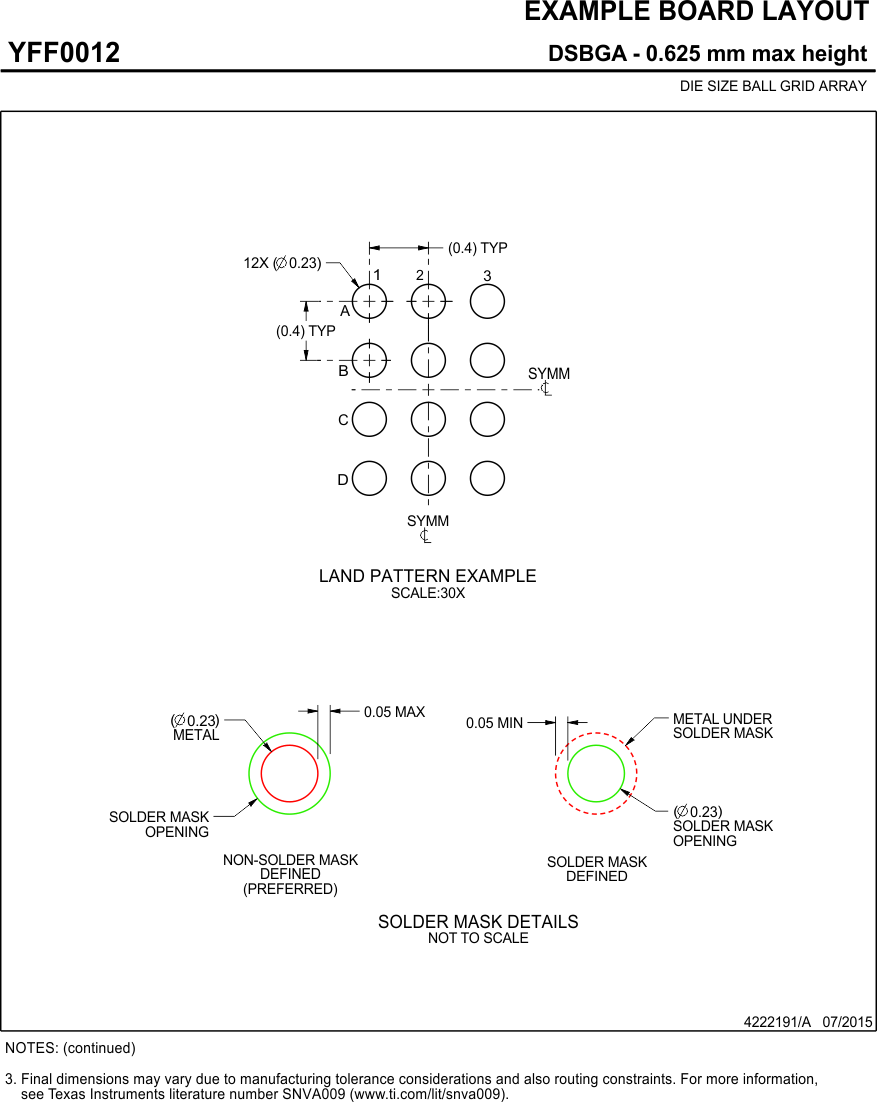
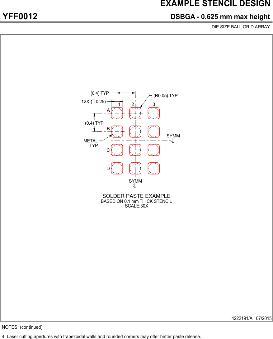
  11. 11Mechanical, Packaging, and Orderable Information

パッケージ・オプション

デバイスごとのパッケージ図は、PDF版データシートをご参照ください。

メカニカル・データ(パッケージ|ピン)
  • YFF|12
  • YFD|12
サーマルパッド・メカニカル・データ
発注情報

Mechanical, Packaging, and Orderable Information

The following pages include mechanical, packaging, and orderable information. This information is the most current data available for the designated devices. This data is subject to change without notice and revision of this document. For browser-based versions of this data sheet, refer to the left-hand navigation.

GUID-80BDAEE9-AA72-4F1D-B9B6-82649BEFEFB5-low.gif
GUID-B4F576C0-5358-483F-9EBC-9D6097AD887D-low.gif
GUID-5E4B58ED-08A0-4F06-BA03-823477A38F79-low.gif
GUID-5ECE4433-9D0D-4C02-909E-A4A7ABFAB0C6-low.gif
GUID-063E3976-E274-437B-9A28-B84FE3B7FCBD-low.gif
GUID-2C510443-BB5C-4BF0-85C6-200C878CA650-low.gif