JAJSEI7E February   2007  – January 2018 INA270 , INA271

PRODUCTION DATA.  

  1. 特長
  2. アプリケーション
  3. 概要
    1.     Device Images
      1.      概略回路図
  4. 改訂履歴
  5. Device Comparison Table
  6. Pin Configuration and Functions
    1.     Pin Functions
  7. Specifications
    1. 7.1 Absolute Maximum Ratings
    2. 7.2 ESD Ratings
    3. 7.3 Recommended Operating Conditions
    4. 7.4 Thermal Information
    5. 7.5 Electrical Characteristics
    6. 7.6 Typical Characteristics
  8. Detailed Description
    1. 8.1 Overview
    2. 8.2 Functional Block Diagram
    3. 8.3 Feature Description
      1. 8.3.1 Basic Connection
      2. 8.3.2 Selecting RS
      3. 8.3.3 Transient Protection
    4. 8.4 Device Functional Modes
      1. 8.4.1 First- or Second-Order Filtering
      2. 8.4.2 Accuracy Variations as a Result of VSENSE and Common-Mode Voltage
        1. 8.4.2.1 Normal Case 1: VSENSE ≥ 20 mV, VCM ≥ VS
        2. 8.4.2.2 Normal Case 2: VSENSE ≥ 20 mV, VCM < VS
        3. 8.4.2.3 Low VSENSE Case 1: VSENSE < 20 mV, –16 V ≤ VCM < 0; and Low VSENSE Case 3: VSENSE < 20 mV, VS < VCM ≤ 80 V
        4. 8.4.2.4 Low VSENSE Case 2: VSENSE < 20 mV, 0 V ≤ VCM ≤ VS
  9. Application and Implementation
    1. 9.1 Application Information
    2. 9.2 Typical Application
      1. 9.2.1 Design Requirements
      2. 9.2.2 Detailed Design Procedure
      3. 9.2.3 Application Curves
  10. 10Power Supply Recommendations
    1. 10.1 Shutdown
  11. 11Layout
    1. 11.1 Layout Guidelines
      1. 11.1.1 RFI and EMI
    2. 11.2 Layout Example
  12. 12デバイスおよびドキュメントのサポート
    1. 12.1 ドキュメントのサポート
      1. 12.1.1 関連資料
    2. 12.2 関連リンク
    3. 12.3 コミュニティ・リソース
    4. 12.4 商標
    5. 12.5 静電気放電に関する注意事項
    6. 12.6 Glossary
  13. 13メカニカル、パッケージ、および注文情報

パッケージ・オプション

メカニカル・データ(パッケージ|ピン)
サーマルパッド・メカニカル・データ
発注情報

Basic Connection

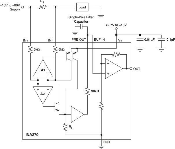
Figure 15 shows the basic connection of the INA270 and INA271. Connect the input pins (IN+ and IN–) as closely as possible to the shunt resistor to minimize any resistance in series with the shunt resistance.

Power-supply bypass capacitors are required for stability. Applications with noisy or high-impedance power supplies may require additional decoupling capacitors to reject power-supply noise. Place minimum bypass capacitors of 0.01 μF and 0.1 μF in value close to the supply pins. Although not mandatory, an additional 10-mF electrolytic capacitor placed in parallel with the other bypass capacitors may be useful in applications with particularly noisy supplies.
INA270 INA271 ai_basic_bos381.gifFigure 15. INA270 Basic Connections