JAJSEI7E February   2007  – January 2018 INA270 , INA271

PRODUCTION DATA.  

  1. 特長
  2. アプリケーション
  3. 概要
    1.     Device Images
      1.      概略回路図
  4. 改訂履歴
  5. Device Comparison Table
  6. Pin Configuration and Functions
    1.     Pin Functions
  7. Specifications
    1. 7.1 Absolute Maximum Ratings
    2. 7.2 ESD Ratings
    3. 7.3 Recommended Operating Conditions
    4. 7.4 Thermal Information
    5. 7.5 Electrical Characteristics
    6. 7.6 Typical Characteristics
  8. Detailed Description
    1. 8.1 Overview
    2. 8.2 Functional Block Diagram
    3. 8.3 Feature Description
      1. 8.3.1 Basic Connection
      2. 8.3.2 Selecting RS
      3. 8.3.3 Transient Protection
    4. 8.4 Device Functional Modes
      1. 8.4.1 First- or Second-Order Filtering
      2. 8.4.2 Accuracy Variations as a Result of VSENSE and Common-Mode Voltage
        1. 8.4.2.1 Normal Case 1: VSENSE ≥ 20 mV, VCM ≥ VS
        2. 8.4.2.2 Normal Case 2: VSENSE ≥ 20 mV, VCM < VS
        3. 8.4.2.3 Low VSENSE Case 1: VSENSE < 20 mV, –16 V ≤ VCM < 0; and Low VSENSE Case 3: VSENSE < 20 mV, VS < VCM ≤ 80 V
        4. 8.4.2.4 Low VSENSE Case 2: VSENSE < 20 mV, 0 V ≤ VCM ≤ VS
  9. Application and Implementation
    1. 9.1 Application Information
    2. 9.2 Typical Application
      1. 9.2.1 Design Requirements
      2. 9.2.2 Detailed Design Procedure
      3. 9.2.3 Application Curves
  10. 10Power Supply Recommendations
    1. 10.1 Shutdown
  11. 11Layout
    1. 11.1 Layout Guidelines
      1. 11.1.1 RFI and EMI
    2. 11.2 Layout Example
  12. 12デバイスおよびドキュメントのサポート
    1. 12.1 ドキュメントのサポート
      1. 12.1.1 関連資料
    2. 12.2 関連リンク
    3. 12.3 コミュニティ・リソース
    4. 12.4 商標
    5. 12.5 静電気放電に関する注意事項
    6. 12.6 Glossary
  13. 13メカニカル、パッケージ、および注文情報

パッケージ・オプション

メカニカル・データ(パッケージ|ピン)
サーマルパッド・メカニカル・データ
発注情報

Shutdown

The INA270 and INA271 do not provide a shutdown pin; however, because these devices consume a quiescent current less than 1 mA, they can be powered by either the output of logic gates or by transistor switches to supply power. Driving the gate low shuts down the INA270 and INA271. Use a totem-pole output buffer or gate that can provide sufficient drive along with a 0.1-μF bypass capacitor, preferably ceramic with good high-frequency characteristics. This gate must have a supply voltage of 3 V or greater because the INA270 and INA271 require a minimum supply greater than 2.7 V. In addition to eliminating quiescent current, this gate also turns off the 10-μA bias current present at each of the inputs. Note that the IN+ and IN– inputs are able to withstand full common-mode voltage under all powered and under-powered conditions. An example shutdown circuit is shown in Figure 22.
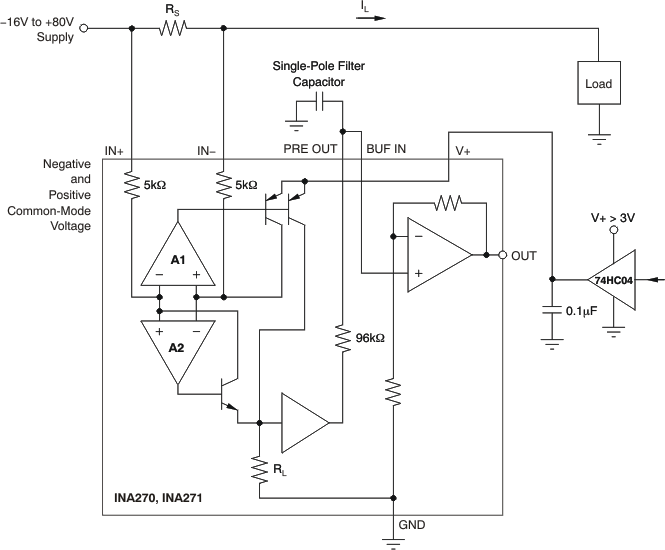
INA270 INA271 ai_cir_shutdown_bos381.gifFigure 22. INA270–INA271 Example Shutdown Circuit