JAJSI53A October   2019  – November 2020 INA290-Q1

PRODUCTION DATA  

  1. 特長
  2. アプリケーション
  3. 概要
  4. Revision History
  5. Pin Configuration and Functions
  6. Specifications
    1. 6.1 Absolute Maximum Ratings
    2. 6.2 ESD Ratings
    3. 6.3 Recommended Operating Conditions
    4. 6.4 Thermal Information
    5. 6.5 Electrical Characteristics
    6. 6.6 Typical Characteristics
  7. Detailed Description
    1. 7.1 Overview
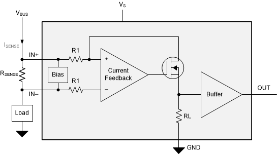
    2. 7.2 Functional Block Diagram
    3. 7.3 Feature Description
      1. 7.3.1 Amplifier Input Common-Mode Range
        1. 7.3.1.1 Input-Signal Bandwidth
        2. 7.3.1.2 Low Input Bias Current
        3. 7.3.1.3 Low VSENSE Operation
        4. 7.3.1.4 Wide Fixed Gain Output
        5. 7.3.1.5 Wide Supply Range
    4. 7.4 Device Functional Modes
      1. 7.4.1 Unidirectional Operation
      2. 7.4.2 High Signal Throughput
  8. Application and Implementation
    1. 8.1 Application Information
      1. 8.1.1 RSENSE and Device Gain Selection
      2. 8.1.2 Input Filtering
    2. 8.2 Typical Application
      1. 8.2.1 Design Requirements
      2. 8.2.2 Detailed Design Procedure
        1. 8.2.2.1 Overload Recovery With Negative VSENSE
      3. 8.2.3 Application Curve
  9. Power Supply Recommendations
  10. 10Layout
    1. 10.1 Layout Guidelines
    2. 10.2 Layout Example
  11. 11Device and Documentation Support
    1. 11.1 Documentation Support
      1. 11.1.1 Related Documentation
    2. 11.2 ドキュメントの更新通知を受け取る方法
    3. 11.3 サポート・リソース
    4. 11.4 Trademarks
    5. 11.5 静電気放電に関する注意事項
    6. 11.6 用語集
  12. 12Mechanical, Packaging, and Orderable Information

パッケージ・オプション

メカニカル・データ(パッケージ|ピン)
サーマルパッド・メカニカル・データ
発注情報

Functional Block Diagram

GUID-20200713-CA0I-G98C-KGNR-5W1HXMP2FDH7-low.gif