JAJSE68 November 2017 INA317
PRODUCTION DATA.
- 1 特長
- 2 アプリケーション
- 3 概要
- 4 改訂履歴
- 5 Pin Configuration and Functions
- 6 Specifications
- 7 Detailed Description
- 8 Application and Implementation
- 9 Power Supply Recommendations
- 10Layout
- 11デバイスおよびドキュメントのサポート
- 12メカニカル、パッケージ、および注文情報
8 Application and Implementation
NOTE
Information in the following applications sections is not part of the TI component specification, and TI does not warrant its accuracy or completeness. TI’s customers are responsible for determining suitability of components for their purposes. Customers should validate and test their design implementation to confirm system functionality.
8.1 Application Information
The INA317 measures small differential voltage with high common-mode voltage that develops between the noninverting and inverting input. The high input impedance makes the INA317 designed for a wide range of applications. The ability to set the reference pin to adjust the functionality of the output signal offers additional flexibility that is practical for multiple configurations.
8.2 Typical Application
Figure 32 shows the basic connections required for operation of the INA317 device. Good layout practice mandates the use of bypass capacitors placed close to the device pins as shown.
The output of the INA317 device is referred to the output reference (REF) pin, which is normally grounded. This connection must be low-impedance to ensure good common-mode rejection. Although 15 Ω or less of stray resistance is tolerated while maintaining specified CMRR, small stray resistances of tens of ohms in series with the REF pin causes noticeable degradation in CMRR.
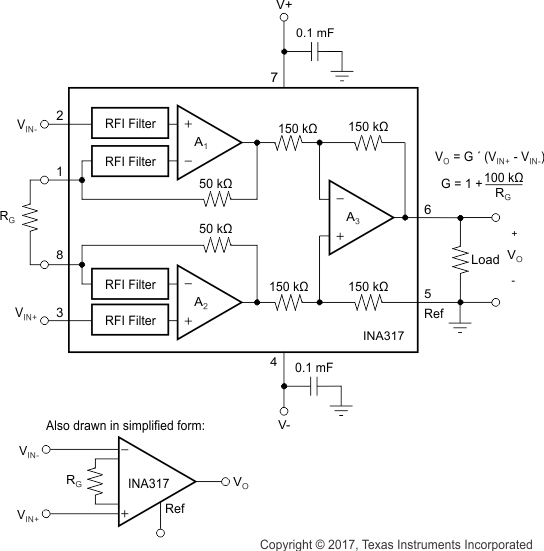 Figure 32. Basic Connections
8.2.1 Design Requirements
The device is configured to monitor the input differential voltage when the gain of the external resistor RG sets the input signal. The output signal references to the REF pin. The most common application is where the output is referenced to ground when no input signal is present by connecting the REF pin to ground. When the input signal increases, the output voltage at the OUT pin increases.
8.2.2 Detailed Design Procedure
8.2.2.1 Setting the Gain
A single external resistor (RG) that is connected between pins 1 and 8 sets the gain of the INA317. The value of RG is selected according to Equation 1:
Table 1 lists several commonly-used gains and resistor values. The 100 kΩ in Equation 1 is a result of the sum of the two internal feedback resistors (A1 and A2.) These on-chip resistors are laser trimmed to accurate absolute values. The accuracy and temperature coefficient of these resistors are included in the gain accuracy and drift specifications of the INA317 device.
The stability and temperature drift of the external gain setting resistor (RG) also affects gain. The contribution of RG to gain accuracy and drift is inferred from the gain inEquation 1. Low resistor values required for high gain make wiring resistance important. Sockets add to the wiring resistance and contribute additional gain error (possibly an unstable gain error) in gains of approximately 100 or greater. To ensure stability, avoid parasitic capacitance of more than a few picofarads at the RG connections. Careful matching of any parasitics on RG pins maintains optimal CMRR over frequency.
Table 1. Commonly-Used Gains and Resistor Values
| DESIRED GAIN | RG (Ω) | NEAREST 1% RG (Ω) |
|---|---|---|
| 1 | NC(1) | NC |
| 2 | 100 k | 100 k |
| 5 | 25 k | 24.9 k |
| 10 | 11.1 k | 11 k |
| 20 | 5.26 k | 5.23 k |
| 50 | 2.04 k | 2.05 |
| 100 | 1.01 k | 1 k |
| 200 | 502.5 | 499 |
| 500 | 200.4 | 200 |
| 1000 | 100.1 | 100 |
8.2.2.2 Internal Offset Correction
The INA317 device internal operational amplifiers use an autocalibration technique with a time-continuous 350-kHz operational amplifier in the signal path. The amplifier is zero-corrected every 8 µs using a proprietary technique. At power-up, the amplifier requires approximately 100 µs to achieve specified VOS accuracy. This design has no aliasing or flicker noise.
8.2.2.3 Offset Trimming
Most applications require no external offset adjustment. However, apply a voltage to the REF pin to make adjustments if necessary. Figure 33 shows an optional circuit for trimming the output offset voltage. The voltage applied to REF pin is added at the output. The operational amplifier buffer provides low impedance at the REF pin to preserve good common-mode rejection.
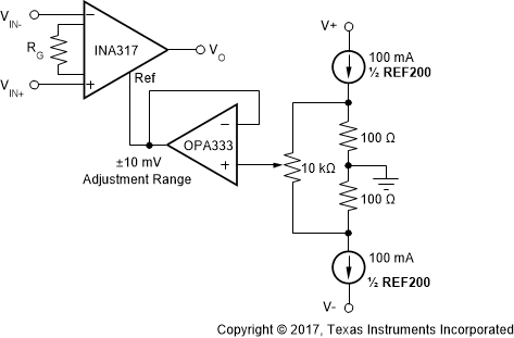 Figure 33. Optional Trimming of Output Offset Voltage
8.2.2.4 Noise Performance
The autocalibration technique used by the INA317 device results in reduced low-frequency noise, typically only 50 nV/√Hz (G = 100). The spectral noise density is shown in Figure 8. Low-frequency noise of the INA317 device is approximately 1 µVPP measured from 0.1 Hz to 10 Hz (G = 100).
8.2.2.5 Input Bias Current Return Path
The input impedance of the INA317 device is extremely high(approximately 100 GΩ.) However, a path must be provided for the input bias current of the inputs. This input bias current is typically ±70 pA. High-input impedance means that this input bias current changes very little with varying input voltage.
For proper operation, input circuitry must provide a path for the input bias current. Figure 34 shows various provisions for an input bias current path. Without a bias current path, the inputs float to a potential that exceeds the common-mode range of the INA317 device, and the input amplifiers saturate. If the differential source resistance is low, the bias current return path connects to one input (see the thermocouple example in Figure 34). With higher source impedance, using two equal resistors provides a balanced input with possible advantages of lower input offset voltage as a result of bias current and better high-frequency common-mode rejection.
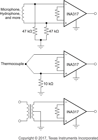 Figure 34. Providing an Input Common-Mode Current Path
8.2.2.6 Input Common-Mode Range
The linear input voltage range of the input circuitry of the INA317 device is from approximately 0.1 V below the positive supply voltage to 0.1 V above the negative supply. As a differential input voltage causes the output voltage to increase, however, the linear input range is limited by the output voltage swing of amplifiers A1 and A2. The linear common-mode input range is related to the output voltage of the complete amplifier. This behavior depends on supply voltage(see Figure 20 to Figure 23 in the Typical Characteristics section.)
Input overload conditions can produce an output voltage that appears normal. For example, if an input overload condition drives both input amplifiers to the respective positive output swing limit, the difference voltage measured by the output amplifier is near zero. The output of the INA317 is near 0 V even though both inputs are overloaded.
8.2.2.7 Operating Voltage
The INA317 operates over a power-supply range of 1.8 V to 5.5 V (±0.9 V to ±2.75 V). Supply voltages higher than 7 V (absolute maximum) can permanently damage the device. Parameters that vary over supply voltage or temperature are shown in the Typical Characteristics section of this data sheet.
8.2.2.8 Low Voltage Operation
The INA317 device operates on power supplies as low as ±0.9 V. Most parameters vary only slightly throughout this supply voltage range; see the Typical Characteristics section. Operation at very low supply voltage requires careful attention to ensure that the input voltages remain within the linear range. Voltage swing requirements of internal nodes limit the input common-mode range with low power supply voltage. Figure 20 to Figure 23 show the range of linear operation for various supply voltages and gains.
8.2.2.9 Single-Supply Operation
The INA317 device can be used on single power supplies of 1.8 V to 5.5 V. Figure 35 shows a basic single-supply circuit. The output REF pin is connected to midsupply. Zero differential input voltage demands an output voltage of midsupply. Actual output voltage swing is limited to approximately 50 mV more than ground when the load is referred to ground as shown. Figure 29 shows how the output voltage swing varies with output current.
With single-supply operation, VIN+ and VIN– must be 0.1 V more than ground for linear operation. For instance, the inverting input cannot connect to ground to measure a voltage that is connected to the noninverting input.
To show the issues affecting low voltage operation, see Figure 35. Figure 35 shows the INA317 device operating from a single 3-V supply. A resistor in series with the low side of the bridge ensures that the bridge output voltage is within the common-mode range of the amplifier inputs.

8.2.2.10 Input Protection
The input pins of the INA317 device are protected with internal diodes that are connected to the power-supply rails. These diodes clamp the applied signal to prevent the signal from damaging the input circuitry. If the input signal voltage exceeds the power supplies by more than 0.3 V, the input signal current must be limited to less than 10 mA to protect the internal clamp diodes. Limit the current with a series input resistor. Some signal sources are inherently current limited and do not require limiting resistors.
8.2.3 Application Curves
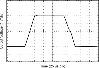
| Gain = 1 | ||

| Gain = 1 | ||
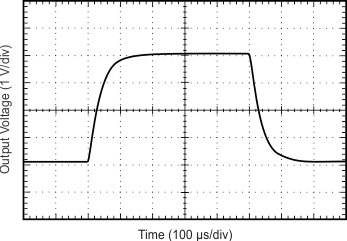
| Gain = 100 | ||
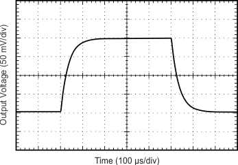
| Gain = 100 | ||