JAJSFX6C August 2018 – July 2019 INA821
PRODUCTION DATA.
- 1 特長
- 2 アプリケーション
- 3 概要
- 4 改訂履歴
- 5 Device Comparison Table
- 6 Pin Configuration and Functions
- 7 Specifications
- 8 Detailed Description
- 9 Application and Implementation
- 10Power Supply Recommendations
- 11Layout
- 12デバイスおよびドキュメントのサポート
- 13メカニカル、パッケージ、および注文情報
パッケージ・オプション
メカニカル・データ(パッケージ|ピン)
サーマルパッド・メカニカル・データ
- DRG|8
発注情報
8.3.1 Setting the Gain
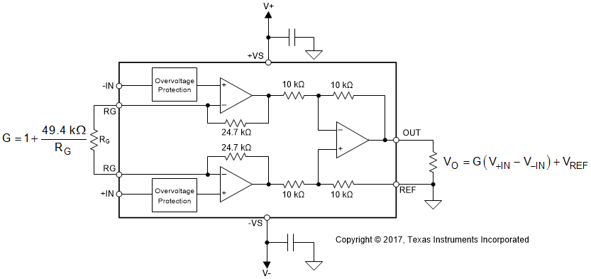
Figure 55 shows that the gain of the INA821 is set by a single external resistor (RG) connected between the RG pins (pins 1 and 8).
 Figure 55. Simplified Diagram of the INA821 With Gain and Output Equations
 The value of RG is selected according to:

Table 2 lists several commonly used gains and resistor values. The 49.4-kΩ term in Equation 1 is a result of the sum of the two internal 24.7-kΩ feedback resistors. These on-chip resistors are laser-trimmed to accurate absolute values. The accuracy and temperature coefficients of these resistors are included in the gain accuracy and drift specifications of the INA821. As shown in Figure 55 and explained in more details in the Layout section, make sure to connect low-ESR, 0.1-µF ceramic bypass capacitors between each supply pin and ground, that are placed as close to the device as possible.
Table 2. Commonly-Used Gains and Resistor Values
| DESIRED GAIN | RG (Ω) | NEAREST 1% RG (Ω) |
|---|---|---|
| 1 | NC | NC |
| 2 | 49.4 k | 49.9 k |
| 5 | 12.35 k | 12.4 k |
| 10 | 5.489 k | 5.49 k |
| 20 | 2.600 k | 2.61 k |
| 50 | 1.008 k | 1 k |
| 100 | 499 | 499 |
| 200 | 248 | 249 |
| 500 | 99 | 100 |
| 1000 | 49.4 | 49.9 |