JAJSFX6C August 2018 – July 2019 INA821
PRODUCTION DATA.
- 1 特長
- 2 アプリケーション
- 3 概要
- 4 改訂履歴
- 5 Device Comparison Table
- 6 Pin Configuration and Functions
- 7 Specifications
- 8 Detailed Description
- 9 Application and Implementation
- 10Power Supply Recommendations
- 11Layout
- 12デバイスおよびドキュメントのサポート
- 13メカニカル、パッケージ、および注文情報
パッケージ・オプション
メカニカル・データ(パッケージ|ピン)
サーマルパッド・メカニカル・データ
- DRG|8
発注情報
8.3.2 EMI Rejection
Texas Instruments developed a method to accurately measure the immunity of an amplifier over a broad frequency spectrum extending from 10 MHz to 6 GHz. This method uses an EMI rejection ratio (EMIRR) to quantify the ability of the INA821 to reject EMI. The offset resulting from an input EMI signal is calculated using Equation 2:

where
- VRF_PEAK is the peak amplitude of the input EMI signal.
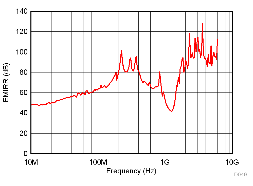
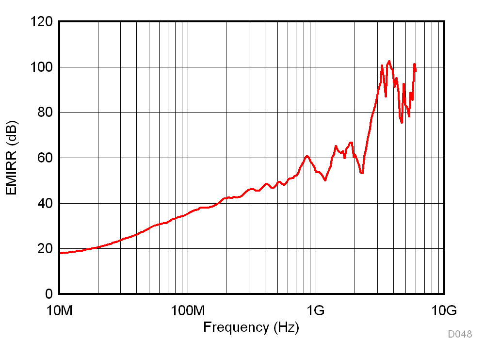
Figure 56 and Figure 57 show the INA821 EMIRR graph for differential and common-mode EMI rejection across this frequency range. Table 3 lists the EMIRR values for the INA821 at frequencies commonly encountered in real-world applications. Applications listed in Table 3 are centered on or operated near the particular frequency shown. Depending on the end-system requirements, additional EMI filters may be required near the signal inputs of the system. Incorporating known good practices such as using short traces, low-pass filters, and damping resistors combined with parallel and shielded signal routing may be required.


Table 3. INA821 EMIRR for Frequencies of Interest
| FREQUENCY | APPLICATION OR ALLOCATION | DIFFERENTIAL EMIRR | COMMON-MODE EM is a result of the sum of the two IRR |
|---|---|---|---|
| 400 MHz | Mobile radio, mobile satellite, space operation, weather, radar, ultrahigh-frequency (UHF) applications | 60 dB | 88 dB |
| 900 MHz | Global system for mobile communications (GSM) applications, radio communication, navigation, GPS (up to 1.6 GHz), GSM, aeronautical mobile, UHF applications | 58 dB | 60 dB |
| 1.8 GHz | GSM applications, mobile personal communications, broadband, satellite,
L-band (1 GHz to 2 GHz) |
66 dB | 89 dB |
| 2.4 GHz | 802.11b, 802.11g, 802.11n, Bluetooth®, mobile personal communications, industrial, scientific and medical (ISM) radio band, amateur radio and satellite, S-band (2 GHz to 4 GHz) | 73 dB | 98 dB |
| 3.6 GHz | Radiolocation, aero communication and navigation, satellite, mobile, S-band | 99 dB | 111 dB |
| 5 GHz | 802.11a, 802.11n, aero communication and navigation, mobile communication, space and satellite operation, C-band (4 GHz to 8 GHz) | 83 dB | 91 dB |