JAJSDR5A August   2017  – January 2018 INA828

PRODUCTION DATA.  

  1. 特長
  2. アプリケーション
  3. 概要
    1.     Device Images
      1.      INA828の簡略化された内部回路図
      2.      入力オフセット電圧ドリフトの代表的な分布
  4. 改訂履歴
  5. Pin Configuration and Functions
    1.     Pin Functions
  6. Specifications
    1. 6.1 Absolute Maximum Ratings
    2. 6.2 ESD Ratings
    3. 6.3 Recommended Operating Conditions
    4. 6.4 Thermal Information
    5. 6.5 Electrical Characteristics
    6. 6.6 Typical Characteristics
  7. Detailed Description
    1. 7.1 Overview
    2. 7.2 Functional Block Diagram
    3. 7.3 Feature Description
      1. 7.3.1 Setting the Gain
        1. 7.3.1.1 Gain Drift
      2. 7.3.2 EMI Rejection
        1. Table 2. INA828 EMIRR for Frequencies of Interest
      3. 7.3.3 Input Common-Mode Range
      4. 7.3.4 Input Protection
      5. 7.3.5 Operating Voltage
    4. 7.4 Device Functional Modes
  8. Application and Implementation
    1. 8.1 Reference Terminal
    2. 8.2 Input Bias Current Return Path
    3. 8.3 PCB Assembly Effects on Precision
    4. 8.4 Typical Application
      1. 8.4.1 Design Requirements
      2. 8.4.2 Detailed Design Procedure
      3. 8.4.3 Application Curves
    5. 8.5 Other Application Examples
      1. 8.5.1 Resistance Temperature Detector Interface
  9. Power Supply Recommendations
  10. 10Layout
    1. 10.1 Layout Guidelines
    2. 10.2 Layout Example
  11. 11デバイスおよびドキュメントのサポート
    1. 11.1 ドキュメントのサポート
      1. 11.1.1 関連資料
    2. 11.2 ドキュメントの更新通知を受け取る方法
    3. 11.3 コミュニティ・リソース
    4. 11.4 商標
    5. 11.5 静電気放電に関する注意事項
    6. 11.6 Glossary
  12. 12メカニカル、パッケージ、および注文情報

パッケージ・オプション

メカニカル・データ(パッケージ|ピン)
サーマルパッド・メカニカル・データ
発注情報

Input Common-Mode Range

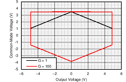
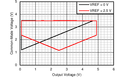
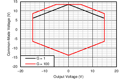
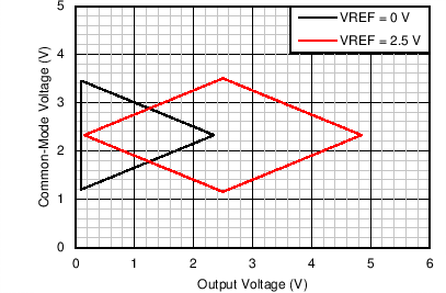
The linear input voltage range of the INA828 input circuitry extends within 2 Volts of both power supplies and maintains excellent common-mode rejection throughout this range. The common-mode range for the most common operating conditions are shown in Figure 55, Figure 50, and Figure 51. The common-mode range for other operating conditions is best calculated using the INA common-mode range calculating tool. The INA828 device can operate over a wide range of power supplies and VREF configurations, thus providing a comprehensive guide to common-mode range limits for all possible conditions is impractical.
INA828 C109_SBOS792.png
VS = 5 V, G = 1
Figure 55. Input Common-Mode Voltage vs Output Voltage
INA828 C110_SBOS792.png
VS = ±5 V, VREF = 0 V
Figure 57. Input Common-Mode Voltage vs Output Voltage
INA828 C112_SBOS792.png
VS = 5 V, G = 100
Figure 56. Input Common-Mode Voltage vs Output Voltage
INA828 C111_SBOS792.png
VS = ±15 V, VREF = 0 V
Figure 58. Input Common-Mode Voltage vs Output Voltage