SLLSFW9 April 2024 ISO7741TA-Q1
ADVANCE INFORMATION
- 1
- 1 Features
- 2 Applications
- 3 Description
- 4 Pin Configuration and Functions
-
5 Specifications
- 5.1 Absolute Maximum Ratings
- 5.2 ESD Ratings
- 5.3 Recommended Operating Conditions
- 5.4 Thermal Information
- 5.5 Power Ratings
- 5.6 Insulation Specifications
- 5.7 Safety-Related Certifications
- 5.8 Safety Limiting Values
- 5.9 Electrical Characteristics Transformer
- 5.10 Electrical Characteristics—5-V Supply
- 5.11 Supply Current Characteristics—5-V Supply
- 5.12 Electrical Characteristics—3.3-V Supply
- 5.13 Supply Current Characteristics—3.3-V Supply
- 5.14 Electrical Characteristics—2.5-V Supply
- 5.15 Supply Current Characteristics—2.5-V Supply
- 5.16 Switching Characteristics—5-V Supply
- 5.17 Switching Characteristics—3.3-V Supply
- 5.18 Switching Characteristics—2.5-V Supply
- 6 Detailed Description
- 7 Application and Implementation
- 8 Device and Documentation Support
- 9 Revision History
- 10Mechanical, Packaging, and Orderable Information
パッケージ・オプション
デバイスごとのパッケージ図は、PDF版データシートをご参照ください。
メカニカル・データ(パッケージ|ピン)
- DW|16
サーマルパッド・メカニカル・データ
発注情報
7.2.2.3 Diode Selection
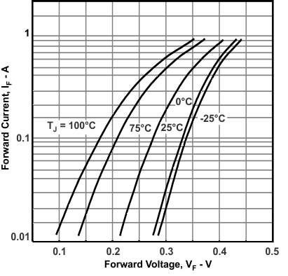
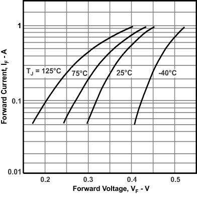
A rectifier diode must always possess low-forward voltage to provide as much voltage to the converter output as possible. When used in high-frequency switching applications, such as the ISO7741Tx-Q1 however, the diode must also possess a short recovery time. Schottky diodes meet both requirements and are therefore strongly recommended in push-pull converter designs. A good choice for low-volt applications and ambient temperatures of up to 85°C is the low-cost Schottky rectifier MBR0520L with a typical forward voltage of 275mV at 100mA forward current. For higher output voltages such as ±10V and above use the MBR0530 which provides a higher DC blocking voltage of 30V.
Lab measurements have shown that at temperatures higher than 100°C the leakage currents of the above Schottky diodes increase significantly. These conditions can cause thermal runaway leading to the collapse of the rectifier output voltage. Therefore, for ambient temperatures higher than 85°C use low-leakage Schottky diodes, such as RB168MM-40.
 Figure 7-2 Diode Forward Characteristics for
MBR0520L
 Figure 7-3 Diode Forward Characteristics MBR0530