JAJSDP1B December 2016 – April 2017 LDC2112 , LDC2114
PRODUCTION DATA.
- 1 特長
- 2 アプリケーション
- 3 概要
- 4 改訂履歴
- 5 概要(続き)
- 6 Pin Configuration and Functions
- 7 Specifications
-
8 Detailed Description
- 8.1 Overview
- 8.2 Functional Block Diagram
- 8.3 Feature Description
- 8.4 Device Functional Modes
- 8.5 Register Maps
-
9 Application and Implementation
- 9.1
Application Information
- 9.1.1 Theory of Operation
- 9.1.2 Designing Sensor Parameters
- 9.1.3 Setting COM Pin Capacitor
- 9.1.4 Defining Power-On Timing
- 9.1.5 Configuring Button Scan Rate
- 9.1.6 Programming Button Sampling Window
- 9.1.7 Scaling Frequency Counter Output
- 9.1.8 Setting Button Triggering Threshold
- 9.1.9 Tracking Baseline
- 9.1.10 Mitigating False Button Detections
- 9.1.11 Reporting Interrupts for Button Presses and Error Conditions
- 9.1.12 Estimating Supply Current
- 9.2 Typical Application
- 9.1
Application Information
- 10Power Supply Recommendations
- 11Layout
- 12デバイスおよびドキュメントのサポート
- 13メカニカル、パッケージ、および注文情報
パッケージ・オプション
メカニカル・データ(パッケージ|ピン)
サーマルパッド・メカニカル・データ
発注情報
11 Layout
11.1 Layout Guidelines
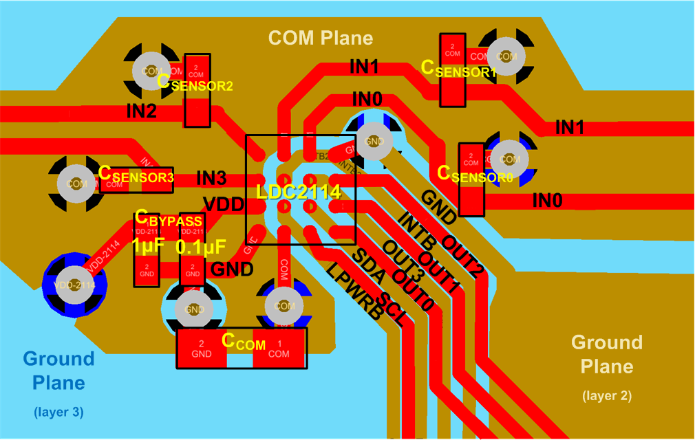
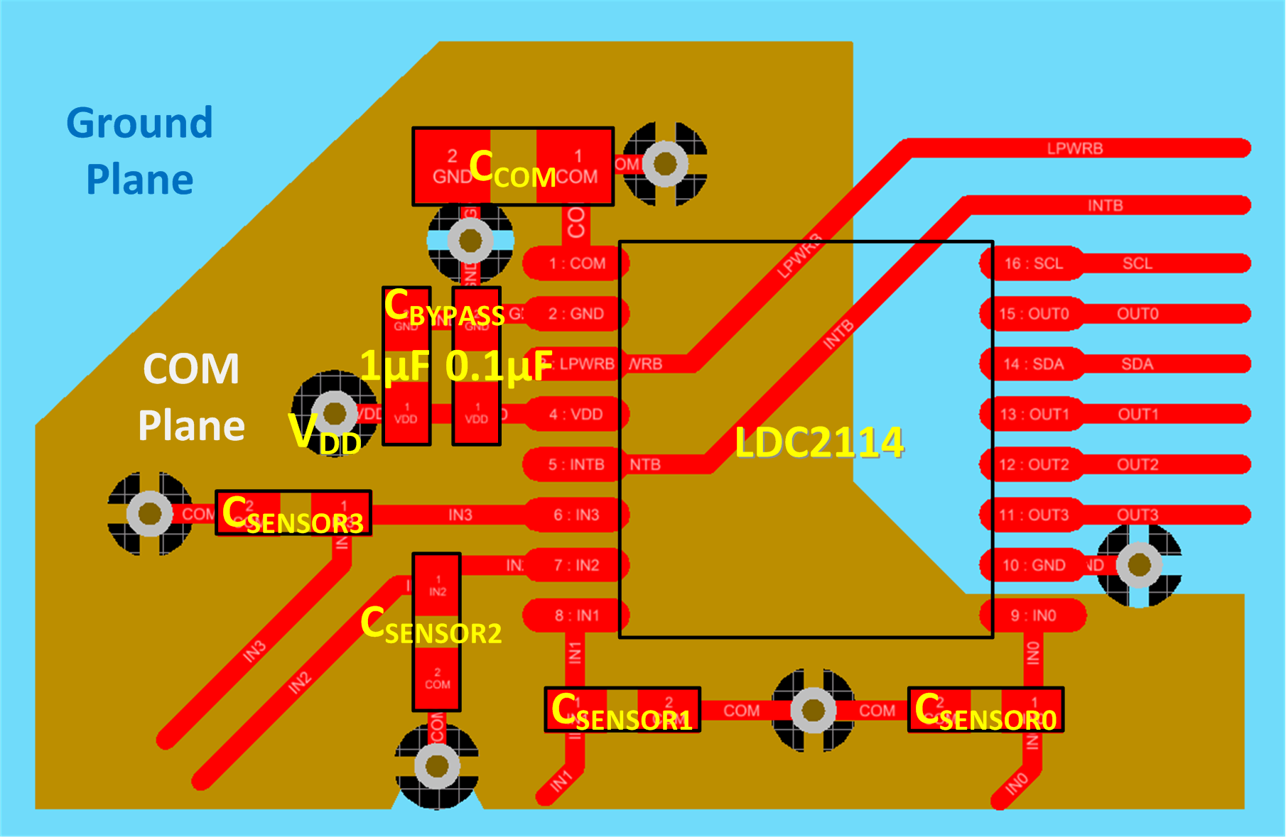
The COM pin must be bypassed to ground with an appropriate value capacitor. For details of how to choose the capacitor value, refer to Setting COM Pin Capacitor. CCOM should be placed as close as possible to the COM pin. The COM signal should be tied to a small copper fill placed underneath the INn signals. The INn signals should stay clear of other high frequency traces.
Each active channel needs to have an LC resonator connected to the corresponding INn pins. The sensor capacitor should be placed within 10 mm of the corresponding INn pin, and the inductor (NOT shown in Figure 32) should be placed at the appropriate location next to (but not touching) the metal target. The INn traces should be at least 6 mil (0.15 mm) wide to minimize parasitic inductances.
For the DSBGA package, the inner four device pads (INTB, OUT3, LPWRB, and SDA) should be routed out on an inner layer through vias, with the traces offset to reduce coupling with other signals. These four vias may need to use blind vias or microvias to bring the signals out. The PCB layer stack should use a thinner (4 mil or 0.1 mm thickness) dielectric between the top copper and next copper layer so that microvias can be used.
11.2 Layout Example
 Figure 32. Layout of LDC2114 (DSBGA-16) With Decoupling Capacitors and Sensor Capacitors
 Figure 33. Layout of LDC2114 (TSSOP-16) With Decoupling Capacitors and Sensor Capacitors
11.3 DSBGA Light Sensitivity
Exposing the DSBGA device to direct light may cause incorrect operation of the device. Light sources such as halogen lamps can affect electrical performance if they are situated in proximity to the device. Light with wavelengths in the red and infrared part of the spectrum have the most detrimental effect.