JAJSDP1B December 2016 – April 2017 LDC2112 , LDC2114
PRODUCTION DATA.
- 1 特長
- 2 アプリケーション
- 3 概要
- 4 改訂履歴
- 5 概要(続き)
- 6 Pin Configuration and Functions
- 7 Specifications
-
8 Detailed Description
- 8.1 Overview
- 8.2 Functional Block Diagram
- 8.3 Feature Description
- 8.4 Device Functional Modes
- 8.5 Register Maps
-
9 Application and Implementation
- 9.1
Application Information
- 9.1.1 Theory of Operation
- 9.1.2 Designing Sensor Parameters
- 9.1.3 Setting COM Pin Capacitor
- 9.1.4 Defining Power-On Timing
- 9.1.5 Configuring Button Scan Rate
- 9.1.6 Programming Button Sampling Window
- 9.1.7 Scaling Frequency Counter Output
- 9.1.8 Setting Button Triggering Threshold
- 9.1.9 Tracking Baseline
- 9.1.10 Mitigating False Button Detections
- 9.1.11 Reporting Interrupts for Button Presses and Error Conditions
- 9.1.12 Estimating Supply Current
- 9.2 Typical Application
- 9.1
Application Information
- 10Power Supply Recommendations
- 11Layout
- 12デバイスおよびドキュメントのサポート
- 13メカニカル、パッケージ、および注文情報
パッケージ・オプション
メカニカル・データ(パッケージ|ピン)
サーマルパッド・メカニカル・データ
発注情報
7 Specifications
7.1 Absolute Maximum Ratings
Over operating temperature range unless otherwise noted.(1)| MIN | MAX | UNIT | ||
|---|---|---|---|---|
| VDD | Supply voltage | 2.2 | V | |
| VI | Voltage on SCL, SDA | –0.3 | 3.6 | V |
| Voltage on any other pin | –0.3 | 2.2(2) | V | |
| TJ | Junction temperature | –40 | 85 | ℃ |
| TSTG | Storage temperature | –65 | 125 | °C |
7.2 ESD Ratings
| VALUE | UNIT | |||
|---|---|---|---|---|
| V(ESD) | Electrostatic discharge | Human body model (HBM), per ANSI/ESDA/JEDEC JS-001(1) | ±1000 | V |
| Charged device model (CDM), per JEDEC specification JESD22-C101(2) | ±250 | |||
7.3 Recommended Operating Conditions
Over operating temperature range unless otherwise noted.| MIN | NOM | MAX | UNIT | ||
|---|---|---|---|---|---|
| VDD | Supply voltage | 1.71 | 1.89 | V | |
| TJ | Junction temperature | –40 | 85 | °C | |
7.4 Thermal Information
| THERMAL METRIC(1) | LDC2112/LDC2114 | UNIT | ||
|---|---|---|---|---|
| DSBGA | TSSOP | |||
| 16 PINS | 16 PINS | |||
| RθJA | Junction-to-ambient thermal resistance | 81.8 | 105.1 | °C/W |
| RθJC(top) | Junction-to-case (top) thermal resistance | 0.4 | 40.3 | °C/W |
| RθJB | Junction-to-board thermal resistance | 18.2 | 50.2 | °C/W |
| ΨJT | Junction-to-top characterization parameter | 0.3 | 3.6 | °C/W |
| ΨJB | Junction-to-board characterization parameter | 18 | 49.6 | °C/W |
7.5 Electrical Characteristics
Over operating temperature range unless otherwise noted. VDD = 1.8 V, TJ = 25 °C.| PARAMETER | TEST CONDITIONS | MIN | TYP | MAX | UNIT | |
|---|---|---|---|---|---|---|
| POWER | ||||||
| VDD | Supply voltage | 1.71 | 1.8 | 1.89 | V | |
| IDDNP | Normal power mode supply current (4 channels)(1)(2)(3) | 4 channels, 40 SPS per channel, 1 ms sampling window per channel, LPWRB = VDD |
0.49 | mA | ||
| IDDNP | Normal power mode supply current (2 channels)(1)(2) | 2 channels, 40 SPS per channel, 1 ms sampling window per channel, LPWRB = VDD |
0.26 | mA | ||
| IDDLP | Low power mode supply current(1)(2) | 1 channel, 1.25 SPS per channel, 1 ms sampling window per channel, LPWRB = Ground |
9 | µA | ||
| IDDSB | Standby supply current | No button active (EN = 0x00) | 5 | 7 | µA | |
| SENSOR | ||||||
| ISENSOR, MAX | Sensor maximum current drive | Registers SENSORn_CONFIG: RPn = 0 (4) | 2.5 | mA | ||
| RP, MIN | Sensor minimum parallel resonant impedance | 350 | Ω | |||
| RP, MAX | Sensor maximum parallel resonant impedance | 10 | kΩ | |||
| fSENSOR | Sensor resonant frequency | 1 | 30 | MHz | ||
| QSENSOR, MIN | Sensor minimum quality factor | 5 | ||||
| QSENSOR, MAX | Sensor maximum quality factor | 30 | ||||
| VSENSOR, PP | Sensor oscillation peak-to-peak voltage | Measured on the INn(4) pins with reference to COM. | 0.9 | V | ||
| CIN | Sensor input pin capacitance | 17 | pF | |||
| CONVERTER | ||||||
| SRNP, MIN | Minimum normal power mode scan rate(5) | LPWRB = VDD | 7 | 10 | 13 | SPS |
| SRNP, MAX | Maximum normal power mode scan rate(5) | LPWRB = VDD | 56 | 80 | 104 | SPS |
| SRLP, MIN | Minimum low power mode scan rate(5) | LPWRB = Ground | 0.438 | 0.625 | 0.813 | SPS |
| SRLP, MAX | Maximum low power mode scan rate(5) | LPWRB = Ground | 3.5 | 5 | 6.5 | SPS |
| Resolution | Data code width | 12 | Bits | |||
7.6 Digital Interface
Over operating temperature range unless otherwise noted. VDD = 1.8 V, TJ = 25 °C. Pins: LPWRB, INTB, OUT0, OUT1, OUT2, OUT3, and ADDR.| PARAMETER | TEST CONDITIONS | MIN | TYP | MAX | UNIT | |
|---|---|---|---|---|---|---|
| VOLTAGE LEVELS | ||||||
| VIH | Input high voltage | 0.8 × VDD | V | |||
| VIL | Input low voltage | 0.2 × VDD | V | |||
| VOH | Output high voltage | ISOURCE = 400 µA | 0.8 × VDD | V | ||
| VOL | Output low voltage | ISINK = 400 µA | 0.2 × VDD | V | ||
| IL | Digital input leakage current | –500 | 500 | nA | ||
7.7 I2C Interface
| MIN | TYP | MAX | UNIT | |||
|---|---|---|---|---|---|---|
| VOLTAGE LEVELS | ||||||
| VIH | Input high voltage | 0.7 × VDD | V | |||
| VIL | Input low voltage | 0.3 × VDD | V | |||
| VOL | Output low voltage | 3 mA sink current | 0.2 × VDD | V | ||
| HYS | Hysteresis(1) | 0.05 × VDD | V | |||
| I2C TIMING CHARACTERISTICS | ||||||
| fSCL | Clock frequency | 400 | kHz | |||
| tLOW | Clock low time | 1.3 | µs | |||
| tHIGH | Clock high time | 0.6 | µs | |||
| tHD;STA | Hold time repeated START condition | After this period, the first clock pulse is generated. | 0.6 | µs | ||
| tSU;STA | Set-up time for a repeated START condition | 0.6 | µs | |||
| tHD;DAT | Data hold time | 0 | µs | |||
| tSU;DAT | Data set-up time | 100 | ns | |||
| tSU;STO | Set-up time for STOP condition | 0.6 | µs | |||
| tBUF | Bus free time between a STOP and START condition | 1.3 | µs | |||
| tVD;DAT | Data valid time | 0.9 | µs | |||
| tVD;ACK | Data valid acknowledge time | 0.9 | µs | |||
| tSP | Pulse width of spikes that must be suppressed by the input filter(1) | 50 | ns | |||
 Figure 1. I2C Timing Diagram
7.8 Typical Characteristics
Over recommended operating conditions unless specified otherwise. VDD = 1.8 V, TJ = 25 °C. One channel enabled with a button sampling window of 1 ms unless specified otherwise.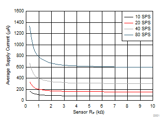 Figure 2. Supply Current vs Sensor RP for Normal Power Mode. Sensor Frequency = 3.6 MHz. Four Channels Enabled.
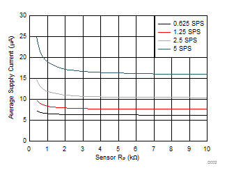 Figure 4. Supply Current vs Sensor RP for Low Power Mode. Sensor Frequency = 3.6 MHz.
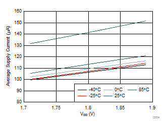 Figure 6. Supply Current vs VDD. Sensor RP = 650 Ω, Scan Rate = 40 SPS.
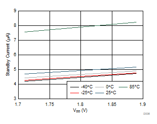 Figure 8. Standby Current vs VDD
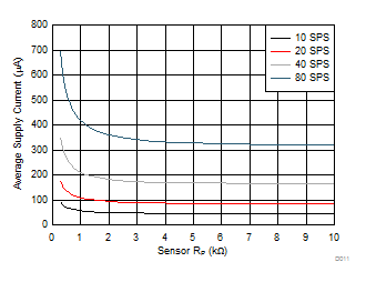 Figure 3. Supply Current vs Sensor RP for Normal Power Mode. Sensor Frequency = 3.6 MHz. Two Channels Enabled.
 Figure 5. Supply Current vs Temperature. Sensor RP = 650 Ω, Scan Rate = 40 SPS.
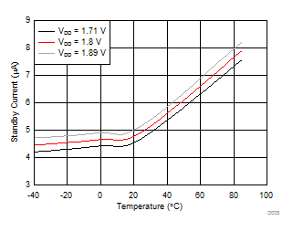 Figure 7. Standby Current vs Temperature
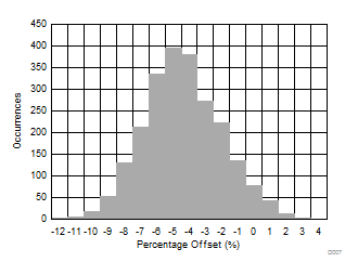 Figure 9. Scan Rate Distribution at 30 °C