SNVS457D February 2007 – October 2015 LM26400Y
PRODUCTION DATA.
1 Features
- Input Voltage Range of 3 V to 20 V
- Dual 2-A Output
- Output Voltage Down to 0.6 V
- Internal Compensation
- 500-kHz PWM Frequency
- Separate Enable Pins
- Separate Soft-Start Pins
- Frequency Foldback Protection
- 175-mΩ NMOS Switch
- Integrated Bootstrap Diodes
- Overcurrent Protection
- HTSSOP and WSON Packages
- Thermal Shutdown
2 Applications
- DTV-LCD
- Set-Top Boxes
- XDSL
- Automotive
- Computing Peripherals
- Industrial Controls
- Points-of-Load
3 Description
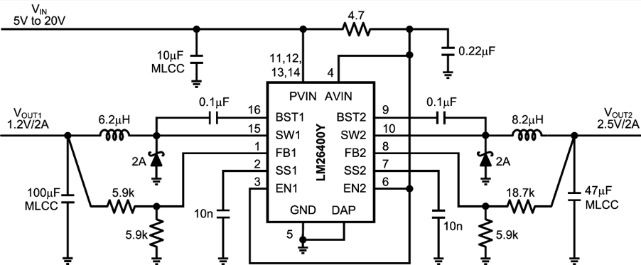
The LM26400Y device is a monolithic, two-output fixed-frequency PWM step-down DC-DC regulator, in a 16-pin WSON or thermally-enhanced HTSSOP package. With a minimum number of external components and internal loop compensation, the LM26400Y is easy to use.
The ability to drive 2-A loads with an internal 175-mΩ NMOS switch using state-of-the-art 0.5-µm BiCMOS technology results in a high-power density design. The world class control circuitry allows for an ON-time as low as 40 ns, thus supporting high-frequency conversion over the entire input range of 3 V to 20 V and down to an output voltage of only 0.6 V. The LM26400Y utilizes peak current-mode control and internal compensation to provide high-performance regulation over a wide range of line and load conditions. Switching frequency is internally set to 500 kHz, optimal for a broad range of applications in terms of size versus thermal tradeoffs.
Given a nonsynchronous architecture, efficiencies above 90% are easy to achieve. External shutdown is included, enabling separate turnon and turnoff of the two channels. Additional features include programmable soft-start circuitry to reduce inrush current, pulse-by-pulse current limit and frequency foldback, integrated bootstrap structure, and thermal shutdown.
Device Information(1)
| PART NUMBER | PACKAGE | BODY SIZE (NOM) |
|---|---|---|
| LM26400Y | WSON (16) | 5.00 mm × 5.00 mm |
| HTSSOP (16) | 4.40 mm × 5.00 mm |
- For all available packages, see the orderable addendum at the end of the data sheet.
Typical Application
