SNVS457D February 2007 – October 2015 LM26400Y
PRODUCTION DATA.
10 Layout
10.1 Layout Guidelines
There are mainly two considerations for PCB layout - thermal and electrical. For thermal details, see Thermal Considerations. Electrical wise, follow the rules below as much as possible. In general, the LM26400Y is a quite robust part in terms of insensitivity to different layout patterns or even abuses.
- Keep the input ceramic capacitor(s) as close to the PVIN pins as possible.
- Use internal ground planes when available.
- The SW pins are high current carrying pins so traces connected to them should be short and fat.
- Keep feedback resistors close to the FB pins.
- Keep the AVIN RC filter close to the AVIN pin.
- Keep the voltage feedback traces away from the switch nodes.
- Use six or more vias next to the ground pad of the catch diode.
- Use at least four vias next to the ground pad of output capacitors.
- Use at least four vias next to each pad of the input capacitors.
For low EMI emission, try not to assign large areas of copper to the noisy switch nodes as a heat sinking method. Instead, assign a lot of copper to the output nodes.
10.1.1 Thermal Shutdown
Whenever the junction temperature of the LM26400Y exceeds 165°C, the MOSFET switch will be kept off until the temperature drops below 150°C, at which point the regulator will go through a hard start to quickly raise the output voltage back to normal. Since it is a hard start, there will be an overshoot at the output. See Figure 20.
10.1.2 Power Loss Estimation
The total power loss in the LM26400Y comprises of three parts: the power FET conduction loss, the power FET switching loss, and the IC's housekeeping power loss. Use Equation 10 to estimate the conduction loss.

where
- TJ is the junction temperature or the target junction temperature if the former is unknown
- RDS is the ON resistance of the internal FET at room temperature
Use 180 mΩ for RDS if the actual value is unknown.
Use Equation 11 to estimate the switching loss.

Another loss in the IC is the housekeeping loss. The loss is the power dissipated by circuitry in the IC other than the power FETs. The equation is:

The 15 mW is gate drive loss. Do the calculation for both channels and find out the total power loss in the IC.

The power loss calculation can help estimate the overall power supply efficiency.
Example:
VIN = 12 V, VOUT1 = 1.2 V, IOUT1 = 2 A, VOUT2 = 2.5 V, IOUT2 = 2 A. Target junction temperature is 90°C.
So conduction loss in Channel 1 is:

Conduction loss in Channel 2 is:

Switching loss in either channel is:

Housekeeping loss is:

Finally the total power loss in the LM26400Y is:

10.1.3 Inductor Selection
TI recommends an inductance value that gives a peak-to-peak ripple current of 0.4 A to 0.8 A. Too large of a ripple current can reduce the maximum achievable DC load current because the peak current of the switch is limited to a typical of 3 A. Too small of a ripple current can cause the regulator to oscillate due to the lack of inductor current ramp signal, especially under high input voltages. Use Equation 19 to determine inductance:

where
- VIN_MAX is the maximum input voltage of the application.
The rated current of the inductor should be higher than the maximum DC load current. Generally speaking, the lower the DC resistance of the inductor winding, the higher the overall regulator efficiency.
Ferrite core inductors are recommended for less AC loss and less fringing magnetic flux. The drawback of ferrite core inductors is their quick saturation characteristic. Once the inductor gets saturated, its current can spike up very quickly if the switch is not turned off immediately. The current limit circuit has a propagation delay and so is oftentimes not fast enough to stop the saturated inductor from going above the current limit. This has the potential to damage the internal switch. So to prevent a ferrite core inductor from getting into saturation, the inductor saturation current rating should be higher than the switch current limit ICL. The LM26400Y is quite robust in handling short pulses of current that is a few amps above the current limit. When a compromise has to be made, pick an inductor with a saturation current just above the lower limit of the ICL. Be sure to validate the short-circuit protection over the intended temperature range.
To prevent the inductor from saturating over the entire –40°C to 125°C range, pick one with a saturation current higher than the upper limit of ICL in Electrical Characteristics.
Inductor saturation current is usually lower when hot. So consult the inductor vendor if the saturation current rating is only specified at room temperature.
Soft saturation inductors such as the iron powder types can also be used. Such inductors do not saturate suddenly and therefore are safer when there is a severe overload or even shorted output. Their physical sizes are usually smaller than the Ferrite core inductors. The downside is their fringing flux and higher power dissipation due to relatively high AC loss, especially at high frequencies.
Example:
VOUT = 1.2 V; VIN = 9 V to 14 V; IOUT = 2 A maximum; Peak-to-peak Ripple Current ΔI = 0.6 A.

Choose a 5-µH or so ferrite core inductor that has a saturation current around 3 A at room temperature. For example, Sumida's CDRH6D26NP-5R0NC.
If the maximum load current is significantly lower than 2 A, pick an inductor with the same saturation rating as a 2-A design but with a lowered DC current rating. That should result in a smaller inductor. There are not many choices, though. Another possibility is to use a soft saturation type inductor, whose size will be dominated by the DC current rating.
10.1.4 Output Capacitor Selection
Output capacitors in a buck regulator handles the AC current from the inductor and so have little ripple RMS current and their power dissipation is not a concern. The concern usually revolves around loop stability and capacitance retention.
The LM26400Y's internal loop compensation was designed around ceramic output capacitors. From a stability point of view, the lower the output voltage, the more capacitance is needed.
Below is a quick summary of temperature characteristics of some commonly used ceramic capacitors. So an X7R ceramic capacitor means its capacitance can vary ±15% over the temperature range of –55°C to 125°C.
Table 4. Capacitance Variation Over Temperature (Class II Dielectric Ceramic Capacitors)
| LOW TEMPERATURE | HIGH TEMPERATURE | CAPACITANCE CHANGE RANGE |
|---|---|---|
| X: –55°C | 5: +85°C | R: ±15% |
| Y: –30°C | 6: +105°C | S: ±22% |
| Z: +10°C | 7: +125°C | U: +22%, –56% |
| 8: +150°C | V: +22%, –82% |
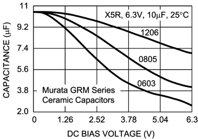
Besides the variation of capacitance over temperature, the actual capacitance of ceramic capacitors also vary, sometimes significantly, with applied DC voltage. Figure 34 illustrates such a characteristic of several ceramic capacitors of various physical sizes from Murata. Unless the DC voltage across the capacitor is going to be small relative to its rated value, going to too small a physical size will have the penalty of losing significant capacitance during circuit operation.
 Figure 34. Capacitance vs Applied DC Voltage
The amount of output capacitance directly contributes to the output voltage ripple magnitude. A quick way to estimate the output voltage ripple is to multiply the inductor peak-to-peak ripple current by the impedance of the output capacitors. For example, if the inductor ripple current is 0.6 A peak-to-peak, and the output capacitance is 44 µF, then the output voltage ripple should be close to 0.6 A × (6.28 × 500 kHz × 44 µF)-1 = 4.3 mV. Sometimes when a large ceramic capacitor is used, the switching frequency may be higher than the capacitor's self resonance frequency. In that case, find out the true impedance at the switching frequency and then multiply that value by the ripple current to get the ripple voltage.
The amount of output capacitance also impacts the stability of the feedback loop. Refer to Loop Stability for guidelines.
10.1.5 Input Capacitor Selection
The input capacitors provide the AC current needed by the nearby power switch so that current provided by the upstream power supply does not carry a lot of AC content, generating less EMI. To the buck regulator in question, the input capacitor also prevents the drain voltage of the FET switch from dipping when the FET is turned on, therefore providing a healthy line rail for the LM26400Y to work with. Since typically most of the AC current is provided by the local input capacitors, the power loss in those capacitors can be a concern. In the case of the LM26400Y regulator, since the two channels operate 180° out of phase, the AC stress in the input capacitors is less than if they operated in phase. The measure for the AC stress is called input ripple RMS current. It is strongly recommended that at least one 4.7-µF ceramic capacitor be placed next to the PVIN pins. Bulk capacitors such as electrolytic capacitors or OSCON capacitors can be added to help stabilize the local line voltage, especially during large load transient events. As for the ceramic capacitors, use X7R , X6S, or X5R types. They maintain most of their capacitance over a wide temperature range. Try to avoid sizes smaller than 0805. Otherwise significant drop in capacitance may be caused by the DC bias voltage. See Output Capacitor Selection section for more information. The DC voltage rating of the ceramic capacitor should be higher than the highest input voltage.
Capacitor temperature is a major concern in board designs. While using a 4.7-µF or higher MLCC as the input capacitor is a good starting point, it is a good idea to check the temperature in the real thermal environment to make sure the capacitors are not over heated. Capacitor vendors may provide curves of ripple RMS current versus temperature rise, based on a designated thermal impedance. In reality, the thermal impedance may be very different. So it is always a good idea to check the capacitor temperature on the board.
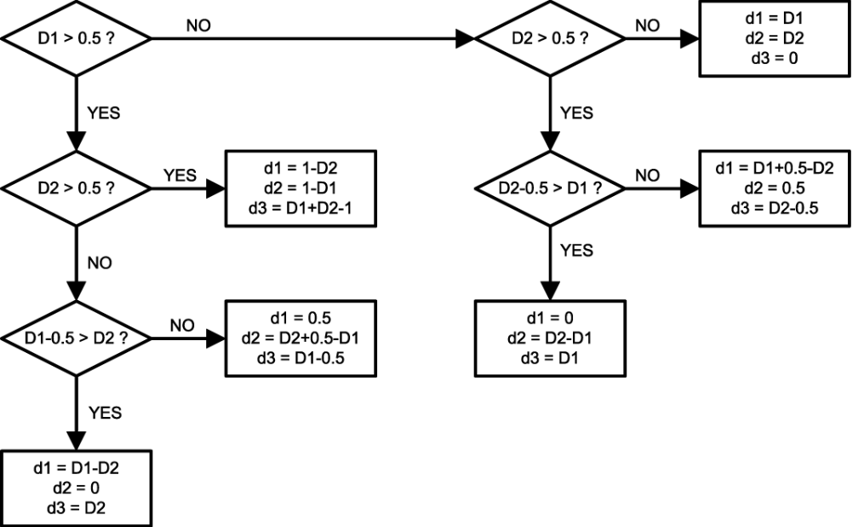
Because the duty cycles of the two channels may overlap, calculation of the input ripple RMS current is a little tedious. Use Equation 21:

where
- I1 is Channel 1's maximum output current
- I2 is Channel 2's maximum output current
- d1 is the non-overlapping portion of Channel 1's duty cycle, D1
- d2 is the non-overlapping portion of Channel 2's duty cycle, D2
- d3 is the overlapping portion of the two duty cycles
- Iav is the average input current, Iav= I1 × D1 + I2 × D2
To quickly determine the values of d1, d2, and d3, refer to the decision tree in Figure 35. To determine the duty cycle of each channel, use D = VOUT/VIN for a quick result or use the following equation for a more accurate result.

where
- RDC is the winding resistance of the inductor
- RDS is the ON-resistance of the MOSFET switch.
Example:
VIN = 5 V, VOUT1 = 3.3 V, IOUT1 = 2 A, VOUT2 = 1.2 V, IOUT2 = 1.5 A, RDS = 170 mΩ, RDC = 30 mΩ. (IOUT1 is the same as I1 in the input ripple RMS current equation, IOUT2 is the same as I2).
First, find out the duty cycles. Plug the numbers into the duty cycle equation and we get D1 = 0.75, and D2 = 0.33. Next, follow the decision tree in Figure 35 to find out the values of d1, d2, and d3. In this case, d1 = 0.5, d2 = D2 + 0.5 – D1 = 0.08, and d3 = D1 – 0.5 = 0.25. Iav = IOUT1 × D1 + IOUT2 × D2 = 1.995 A. Plug all the numbers into the input ripple RMS current equation and the result is Iirrm = 0.77 A.
 Figure 35. Determining d1, d2, and d3
10.1.6 Catch Diode Selection
The catch diode should be at least 2-A rated. The most stressful operation for the diode is usually when the output is shorted under high line. Always pick a Schottky diode for its lower forward drop and higher efficiency. The reverse voltage rating of the diode should be at least 25% higher than the highest input voltage. The diode junction temperature is a main concern here. Always validate the diode's junction temperature in the intended thermal environment to make sure its thermally derated maximum current is not exceeded. There are a few 2-A, 30-V surface mount Schottky diodes available in the market. Diodes have a negative temperature coefficient, so do not put two diodes in parallel to achieve a lower temperature rise. Current will be hogged by one of the diodes instead of shared by the two. Use a larger package for that purpose.
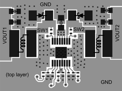
10.2 Layout Example
 Figure 36. PCB Layout Example
10.3 Thermal Considerations
Due to the low thermal impedance from junction to the die-attach pad (or DAP, exposed metal at the bottom of the package), thermal performance heavily depends on PCB copper arrangement. The minimum requirement is to have a top-layer thermal pad that is exactly the same size as the DAP. There should be at least nine 8-mil thermal vias in the pad. The thermal vias should be connected to internal ground planes (if available) and to a ground plane on the bottom layer that is as large as allowed.
In boards that have internal ground planes, extending the top-layer thermal pad outside the body of the package to form a "dogbone" shape offers little performance improvement. However, for two-layer boards, the dogbone shape on the top layer will provide significant help.
Predicting on paper with reasonable accuracy the junction temperature of the LM26400Y in a real-world application is still an art. Major factors that contribute to the junction temperature but not directly associated with the thermal performance of the LM26400Y itself include air speed, air temperature, nearby heating elements and arrangement of PCB copper connected to the DAP of the LM26400Y. The RθJA value published in the datasheet is based on a standard board design in a single heating element mode and measured in a standard environment. The real application is usually completely different from those conditions. So the actual RθJA will be significantly different from the datasheet number. The best approach is still to assign as much copper area as allowed to the DAP and prototype the design.
When prototyping the design, it is necessary to know the junction temperature of the LM26400Y to assess the thermal margin. The best way to measure the LM26400Y's junction temperature when the board is working in its usual mode is to measure the package-top temperature using an infrared thermal imaging camera. Look for the highest temperature reading across the case-top. Add two degrees to the measurement result and the number should be a pretty good estimate of the junction temperature. Due to the high temperature gradient across the case-top, the use of a thermal couple is generally not recommended. If a thermal couple has to be used, try to locate the hottest spot on the case-top first and then secure the thermal couple at exactly the same location. The thermal couple needs to be a light-gauge type (such as 40-gauge). Apply a small blob of thermal compound to the contact point and then secure the thermal couple on the case-top using thermally non-conductive glue.
If the maximum allowed junction temperature is exceeded, load current has to be lowered to bring the temperature back in specification. Or better thermal management such as more air flow needs to be provided.
As a summary, here is a list of important items to consider:
- Use multi-layer PC boards with internal ground planes.
- Use nine or more thermal vias to connect the top-layer thermal pad to internal ground planes and ground copper on the bottom layer.
- Generate as large a ground plane as allowable on outer layers, especially near the package.
- Use 2-oz. copper whenever possible.
- Try to spread out heat generating components.
- The inductors and diodes are heat generating components and should be connected to power or ground planes using many vias.