JAJSAY2G September 2008 – September 2015 LM3150
PRODUCTION DATA.
- 1 特長
- 2 アプリケーション
- 3 概要
- 4 改訂履歴
- 5 Pin Configuration and Functions
- 6 Specifications
- 7 Detailed Description
- 8 Application and Implementation
- 9 Power Supply Recommendations
- 10Layout
- 11デバイスおよびドキュメントのサポート
- 12メカニカル、パッケージ、および注文情報
パッケージ・オプション
メカニカル・データ(パッケージ|ピン)
- PWP|14
サーマルパッド・メカニカル・データ
- PWP|14
発注情報
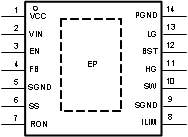
5 Pin Configuration and Functions
HTSSOP PWP
14 PINS
Top View

Pin Functions
| PIN | I/O | DESCRIPTION | FUNCTION | |
|---|---|---|---|---|
| NAME | NO. | |||
| VCC | 1 | O | Supply Voltage for FET Drivers | Nominally regulated to 5.95 V. Connect a 1.0-µF to 4.7-µF decoupling capacitor from this pin to ground. |
| VIN | 2 | I | Input Supply Voltage | Supply pin to the device. Nominal input range is 6 V to 42 V. |
| EN | 3 | I | Enable | To enable the IC, apply a logic high signal to this pin greater than 1.26-V typical or leave floating. To disable the part, ground the EN pin. |
| FB | 4 | I | Feedback | Internally connected to the regulation, overvoltage, and short-circuit comparators. The regulation setting is 0.6 V at this pin. Connect to feedback resistor divider between the output and ground to set the output voltage. |
| SGND | 5,9 | — | Signal Ground | Ground for all internal bias and reference circuitry. Should be connected to PGND at a single point. |
| SS | 6 | I | Soft-Start | An internal 7.7-µA current source charges an external capacitor to provide the soft-start function. |
| RON | 7 | I | On-time Control | An external resistor from VIN to this pin sets the high-side switch on-time. |
| ILIM | 8 | I | Current Limit | Monitors current through the low-side switch and triggers current limit operation if the inductor valley current exceeds a user defined value that is set by RLIM and the Sense current, ILIM-TH, sourced out of this pin during operation. |
| SW | 10 | O | Switch Node | Switch pin of controller and high-gate driver lower supply rail. A boost capacitor is also connected between this pin and BST pin |
| HG | 11 | O | High-Side Gate Drive | Gate drive signal to the high-side NMOS switch. The high-side gate driver voltage is supplied by the differential voltage between the BST pin and SW pin. |
| BST | 12 | I | Connection for Bootstrap Capacitor | High-gate driver upper supply rail. Connect a 0.33 to 0.47-µF capacitor from SW pin to this pin. An internal diode charges the capacitor during the high-side switch off-time. Do not connect to an external supply rail. |
| LG | 13 | O | Low-Side Gate Drive | Gate drive signal to the low-side NMOS switch. The low-side gate driver voltage is supplied by VCC. |
| PGND | 14 | G | Power Ground | Synchronous rectifier MOSFET source connection. Tie to power ground plane. Should be tied to SGND at a single point. |
| EP | — | — | Exposed Pad | Exposed die attach pad should be connected directly to SGND. Also used to help dissipate heat out of the IC. |