JAJSAY2G September 2008 – September 2015 LM3150
PRODUCTION DATA.
- 1 特長
- 2 アプリケーション
- 3 概要
- 4 改訂履歴
- 5 Pin Configuration and Functions
- 6 Specifications
- 7 Detailed Description
- 8 Application and Implementation
- 9 Power Supply Recommendations
- 10Layout
- 11デバイスおよびドキュメントのサポート
- 12メカニカル、パッケージ、および注文情報
パッケージ・オプション
メカニカル・データ(パッケージ|ピン)
- PWP|14
サーマルパッド・メカニカル・データ
- PWP|14
発注情報
8 Application and Implementation
NOTE
Information in the following applications sections is not part of the TI component specification, and TI does not warrant its accuracy or completeness. TI’s customers are responsible for determining suitability of components for their purposes. Customers should validate and test their design implementation to confirm system functionality.
8.1 Application Information
The LM3150 controller employs a COT architecture with ERM (emulated ripple mode) control. This allows for fast transient response, reduction in output voltage ripple, and low external component count. A typical application of this part is described in the following section.
8.2 Typical Application
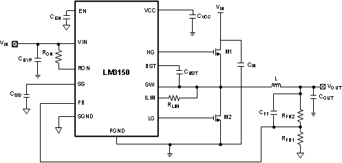 Figure 14. Design Example Schematic
8.2.1 Design Requirements
To properly size the components for the application, the designer needs the following parameters: Input voltage range, output voltage, output current range and required switching frequency. To summarize briefly, these four main parameters will affect the choices of component available to achieve a proper system behavior.
For the power supply, the input impedance of the supply rail should be low enough that the input current transient does not cause drop below the UVLO value. To maintain a relatively constant switching frequency as the input voltage varies, the LM3150 controller automatically adjusts the on-time inversely with the input voltage. The available frequency range for a given input voltage range, is determined by the duty-cycle, D = VOUT/VIN, and the minimum tON and tOFF times. The feedback resistor values can be calculated based on the value of required output and feedback voltage. Regarding the output capacitor, its voltage rating must be greater than or equal to the output voltage. Similarly, the voltage rating for the input capacitor must be greater than the input voltage to be used in the application. Also, a feed-forward capacitor may be required for improved stability, based on the application.
The following sections describe in detail the design requirements for a typical LM3150 application.
8.2.2 Detailed Design Procedure
8.2.2.1 Custom Design with WEBENCH Tools
Click here to create a custom design using the LM3150 device with the WEBENCH® Power Designer.
- Start by entering your VIN, VOUT and IOUT requirements.
- Optimize your design for key parameters like efficiency, footprint and cost using the optimizer dial and compare this design with other possible solutions from Texas Instruments.
- WEBENCH Power Designer provides you with a customized schematic along with a list of materials with real time pricing and component availability.
- In most cases, you will also be able to:
- Run electrical simulations to see important waveforms and circuit performance,
- Run thermal simulations to understand the thermal performance of your board,
- Export your customized schematic and layout into popular CAD formats,
- Print PDF reports for the design, and share your design with colleagues.
- Get more information about WEBENCH tools at www.ti.com/webench.
8.2.2.2 LM3150 Design Procedure
To properly size the components for the application, the designer needs the following parameters: Input voltage range, output voltage, output current range and required switching frequency. These four main parameters will affect the choices of component available to achieve a proper system behavior.
Table 1. Bill of Materials
| DESIGNATOR | VALUE | PARAMETERS | MANUFACTURER | PART NUMBER |
|---|---|---|---|---|
| CBST | 0.47 µF | Ceramic, X7R, 16 V, 10% | TDK | C2012X7R1C474K |
| CBYP | 0.1 µF | Ceramic, X7R, 50 V, 10% | TDK | C2012X7R1H104K |
| CEN | 1000 pF | Ceramic, X7R, 50 V, 10% | TDK | C1608X7R1H102K |
| CFF | 270 pF | Ceramic, C0G, 50 V, 5% | Vishay-Bccomponents | VJ0805A271JXACW1BC |
| CIN1, CIN2 | 10 µF | Ceramic, X5R, 35 V, 20% | Taiyo Yuden | GMK325BJ106KN-T |
| COUT1, COUT2 | 150 µF | Polymer Aluminum, 6.3 V, 20% | Panasonic | EEF-UE0J151R |
| CSS | 0.068 µF | Ceramic, 0805, 25 V, 10% | Vishay | VJ0805Y683KXXA |
| CVCC | 4.7 µF | Ceramic, X7R, 16 V, 10% | Murata | GRM21BR71C475KA73L |
| L1 | 1.65 µH | Shielded Drum Core, 2.53 mΩ | Coilcraft | HA3778–AL |
| M1, M2 | 30 V | 8 nC, RDS(ON) @4.5 V=10 mΩ | Renesas | RJK0305DPB |
| RFB1 | 4.99 kΩ | 1%, 0.125 W | Vishay-Dale | CRCW08054k99FKEA |
| RFB2 | 22.6 kΩ | 1%, 0.125 W | Vishay-Dale | CRCW080522k6FKEA |
| RLIM | 1.91 kΩ | 1%, 0.125 W | Vishay-Dale | CRCW08051K91FKEA |
| RON | 56.2 kΩ | 1%, 0.125 W | Vishay-Dale | CRCW080556K2FKEA |
| U1 | LM3150 | Texas Instruments | LM3150 |
-
Define Power Supply Operating Conditions
- VOUT = 3.3 V
- VIN-MIN = 6 V, VIN-TYP = 12 V, VIN-MAX = 24 V
- Typical Load Current = 12 A, Max Load Current = 15 A
- Soft-Start time tSS = 5 ms
- Set Output Voltage with Feedback Resistors
- Determine RON and fS
-
Determine Inductor Required
- ET = (24-3.3) x (3.3/24) x (1000/500) = 5.7 V µs
- From the inductor nomograph a 12-A load and 5.7 V µs calculation corresponds to a L44 type of inductor.
- Using the inductor designator L44 in Table 2 the Coilcraft HA3778–AL 1.65-µH inductor is chosen.
- Determine Output Capacitance
- Determine Use of Feed-Forward Capacitor
- MOSFET and RLIM Selection
- Calculate Input Capacitance
- Calculate Soft-Start Capacitor
- CVCC, CEN, and CBST


RFB2 = 22.6 kΩ, nearest 1% standard value.
tOFF should meet the following criteria:
At the maximum switching frequency of 687 kHz, which is limited by the minimum on-time, the off-time of 654 ns is less than 725 ns. Therefore the switching frequency should be reduced and meet the following criteria:
A switching frequency is arbitrarily chosen at 500 kHz which should allow for reasonable size components and satisfies the requirements above.
fS = 500 kHz
Using fS = 500 kHz RON can be calculated as follows:
Next, check the desired minimum input voltage for RON using Figure 15. This design will meet the desired minimum input voltage of 6 V.
The voltage rating on the output capacitor should be greater than or equal to the output voltage. As a rule of thumb most capacitor manufacturers suggests not to exceed 90% of the capacitor rated voltage. In the case of multilayer ceramics the capacitance will tend to decrease dramatically as the applied voltage is increased towards the capacitor rated voltage. The capacitance can decrease by as much as 50% when the applied voltage is only 30% of the rated voltage. The chosen capacitor should also be able to handle the rms current which is equal to:

For this design the chosen ripple current ratio, r = 0.3, represents the ratio of inductor peak-to-peak current to load current IOUT. A good starting point for ripple ratio is 0.3 but it is acceptable to choose r between 0.25 to 0.5. The nomographs in this datasheet all use 0.3 as the ripple current ratio.

Minimum output capacitance is:
The maximum ESR allowed to prevent overvoltage protection during normal operation is:
For this design a feed-forward capacitor will be used to help minimize output ripple.
The minimum ESR must meet both of the following criteria:
Based on the above criteria two 150-µF polymer aluminum capacitors with a ESR = 12 mΩ each for a effective ESR in parallel of 6 mΩ was chosen from Panasonic. The part number is EEF-UE0J101P.
From Step 5 the capacitor chosen in ESR is small enough that we should use a feed-forward capacitor. This is calculated from:

Let Cff = 270 pF, which is the closest next standard value.
The LM3150 controller is designed to drive N-channel MOSFETs. For a maximum input voltage of 24 V we should choose N-channel MOSFETs with a maximum drain-source voltage, VDS, greater than 1.2 x 24 V = 28.8 V. FETs with maximum VDS of 30 V will be the first option. The combined total gate charge Qgtotal of the high-side and low-side FET should satisfy the following:
Where IVCCL is the minimum current limit of VCC, over the temperature range, specified in the Electrical Characteristics table. The MOSFET gate charge Qg is gathered from reading the VGS vs Qg curve of the MOSFET datasheet at the VGS = 5 V for the high-side, M1, MOSFET and VGS = 6 V for the low-side, M2, MOSFET.
The Renesas MOSFET RJK0305DPB has a gate charge of 10 nC at VGS = 5 V, and 12 nC at VGS = 6 V. This combined gate charge for a high-side, M1, and low-side, M2, MOSFET 12 nC + 10 nC = 22 nC is less than 130 nC calculated Qgtotal.
The calculated MOSFET power dissipation must be less than the max allowed power dissipation, Pdmax, as specified in the MOSFET data sheet. An approximate calculation of the FET power dissipated Pd, of the high-side and low-side FET is given by:
High-Side MOSFET
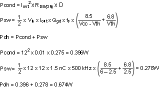
The max power dissipation of the RJK0305DPB is rated as 45 W for a junction temperature that is 125°C higher than the case temperature and a thermal resistance from the FET junction to case, θJC, of 2.78°C/W. When the FET is mounted onto the PCB, the PCB will have some additional thermal resistance such that the total system thermal resistance of the FET package and the PCB, θJA, is typically in the range of 30°C/W for this type of FET package. The max power dissipation, Pdmax, with the FET mounted onto a PCB with a 125°C junction temperature rise above ambient temperature and θJA = 30°C/W, can be estimated by:
The system calculated Pdh of 0.674 W is much less than the FET Pdmax of 4.1 W and therefore the RJK0305DPB max allowable power dissipation criteria is met.
Low-Side MOSFET
Primary loss is conduction loss given by:
Pdl is also less than the Pdmax specified on the RJK0305DPB MOSFET data sheet.
However, it is not always necessary to use the same MOSFET for both the high-side and low-side. For most applications it is necessary to choose the high-side MOSFET with the lowest gate charge and the low-side MOSFET is chosen for the lowest allowed RDS(ON). The plateau voltage of the FET VGS vs Qg curve must be less than VCC - 750 mV.
The current limit resistor, RLIM, is calculated by estimating the RDS(ON) of the low-side FET at the maximum junction temperature of 100°C. By choosing to go into current limit when the average output load current is 20% higher than the output load current of 12A while the inductor ripple current ratio is 1/3 of the load current will make ICL= 10.4 A. Then the following calculation of RLIM is:
Let RLIM = 1.91 kΩ which is the next standard value.
The input capacitor should be chosen so that the voltage rating is greater than the maximum input voltage which for this example is 24 V. Similar to the output capacitor, the voltage rating needed will depend on the type of capacitor chosen. The input capacitor should also be able to handle the input rms current, which is a maximum of approximately 0.5 x IOUT. For this example the rms input current is approximately 0.5 x 12 A = 6 A.
The minimum capacitance with a maximum 5% input ripple ΔVIN-MAX = (0.05 x 12) = 0.6 V:
To handle the large input rms current 2 ceramic capacitors are chosen at 10 µF each with a voltage rating of 50 V and case size of 1210. Each ceramic capacitor is capable of handling 3 A of rms current. A aluminum electrolytic of 5 times the combined input capacitance, 5 x 20 µF = 100 µF, is chosen to provide input voltage filter damping because of the low ESR ceramic input capacitors.
CBYP = 0.1µF ceramic with a voltage rating greater than maximum VIN
The soft start-time should be greater than the input voltage rise time and also satisfy the following equality to maintain a smooth transition of the output voltage to the programmed regulation voltage during startup. The desired soft-start time, tss, of 5 ms also must satisfy the equality in Equation 12, by using the chosen component values through the previous steps as shown below:
Because the desired soft-start time satisfies the equality in Equation 12, the soft start capacitor is calculated as:
Let CSS = 0.068 µF, which is the next closest standard value. This should be a ceramic cap with a voltage rating greater than 10 V.
CVCC = 4.7-µF ceramic with a voltage rating greater than 10 V
CEN = 1000-pF ceramic with a voltage rating greater than 10 V
CBST = 0.47-µF ceramic with a voltage rating greater than 10 V
8.2.2.3 Design Guide
The design guide provides the equations required to design with the LM3150 controller. WEBENCH design tool can be used with or in place of this section for a more complete and simplified design process.
-
Define Power Supply Operating Conditions
- Required Output Voltage
- Maximum and Minimum DC Input Voltage
- Maximum Expected Load Current during Normal Operation
- Soft-Start Time
- Set Output Voltage With Feedback Resistors
- RFB1 is the bottom resistor
- RFB2 is the top resistor
- Determine RON and fs
- Determine Inductor Required Using Figure 16
- fs is in kHz units
- Determine Output Capacitance
- Determine The Use of Feed-Forward Capacitor
- MOSFET and RLIM Selection
- Qgtotal is the combined total gate charge of the high-side and low-side FETs
- Calculate Input Capacitance
- ΔVIN-MAX is the maximum allowable input ripple voltage. A good starting point for the input ripple voltage is 5% of VIN
- Calculate Soft-Start Capacitor
- tss is the soft-start time in seconds
- Vref = 0.6V
- CVCC, CBST, and CEN

where
The available frequency range for a given input voltage range, is determined by the duty-cycle, D = VOUT/VIN, and the minimum tON and tOFF times as specified in the Electrical Characteristics table. The maximum frequency is thus, fsmax = Dmin/tON-MIN. Where Dmin=VOUT/VIN-MAX, is the minimum duty-cycle. The off-time will need to be less than the minimum off-time tOFF as specified in the Electrical Characteristics table plus any turnoff and turnon delays of the MOSFETs which can easily add another 200 ns. The minimum off-time will occur at maximum duty cycle Dmax and will determine if the frequency chosen will allow for the minimum desired input voltage. The requirement for minimum off-time is tOFF= (1–Dmax)/fs ≥ (tOFF-MIN + 200 ns). If tOFF does not meet this requirement it will be necessary to choose a smaller switching frequency fS.
Choose RON so that the switching frequency at your typical input voltage matches your fS chosen above using the following formula:
Use Figure 15 to determine if the calculated RON will allow for the minimum desired input voltage. If the minimum desired input voltage is not met, recalculate RON for a lower switching frequency.
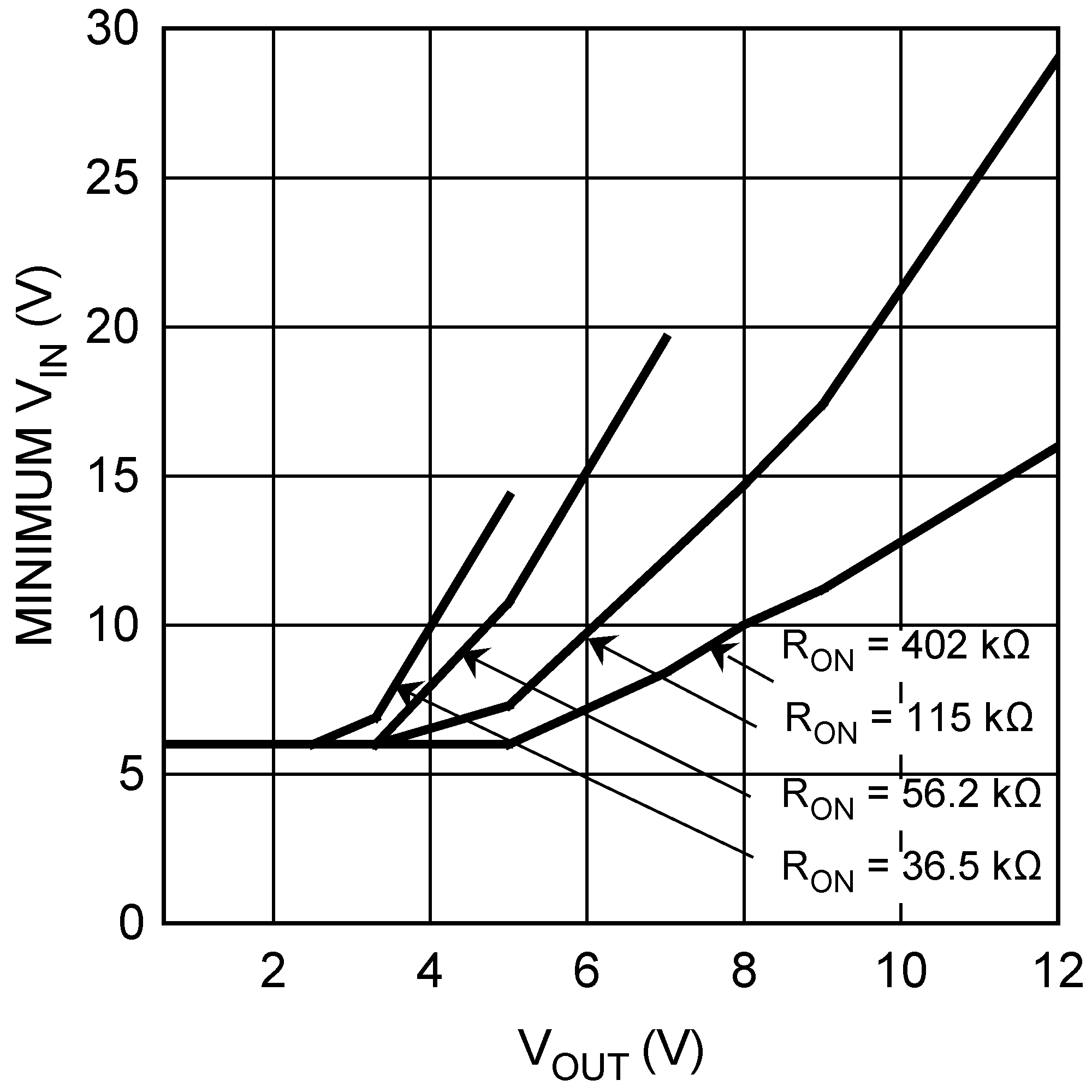 Figure 15. Minimum VIN vs. VOUT
IOUT = 10 A
To use the nomograph in Figure 16, calculate the inductor volt-microsecond constant ET from the following formula:

where
The intersection of the Load Current and the Volt-microseconds lines on the chart below will determine which inductors are capable for use in the design. Figure 16 shows a sample of parts that can be used. The offline calculator tools and WEBENCH will fully calculate the requirements for the components needed for the design.
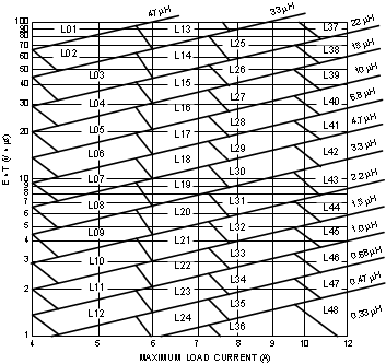 Figure 16. Inductor Nomograph
Table 2. Inductor Selection Table
| INDUCTOR DESIGNATOR | INDUCTANCE (µH) | CURRENT (A) | PART NAME | VENDOR |
|---|---|---|---|---|
| L01 | 47 | 7-9 | ||
| L02 | 33 | 7-9 | SER2817H-333KL | COILCRAFT |
| L03 | 22 | 7-9 | SER2814H-223KL | COILCRAFT |
| L04 | 15 | 7-9 | 7447709150 | WURTH |
| L05 | 10 | 7-9 | RLF12560T-100M7R5 | TDK |
| L06 | 6.8 | 7-9 | B82477-G4682-M | EPCOS |
| L07 | 4.7 | 7-9 | B82477-G4472-M | EPCOS |
| L08 | 3.3 | 7-9 | DR1050-3R3-R | COOPER |
| L09 | 2.2 | 7-9 | MSS1048-222 | COILCRAFT |
| L10 | 1.5 | 7-9 | SRU1048-1R5Y | BOURNS |
| L11 | 1 | 7-9 | DO3316P-102 | COILCRAFT |
| L12 | 0.68 | 7-9 | DO3316H-681 | COILCRAFT |
| L13 | 33 | 9-12 | ||
| L14 | 22 | 9-12 | SER2918H-223 | COILCRAFT |
| L15 | 15 | 9-12 | SER2814H-153KL | COILCRAFT |
| L16 | 10 | 9-12 | 7447709100 | WURTH |
| L17 | 6.8 | 9-12 | SPT50H-652 | COILCRAFT |
| L18 | 4.7 | 9-12 | SER1360-472 | COILCRAFT |
| L19 | 3.3 | 9-12 | MSS1260-332 | COILCRAFT |
| L20 | 2.2 | 9-12 | DR1050-2R2-R | COOPER |
| L21 | 1.5 | 9-12 | DR1050-1R5-R | COOPER |
| L22 | 1 | 9-12 | DO3316H-102 | COILCRAFT |
| L23 | 0.68 | 9-12 | ||
| L24 | 0.47 | 9-12 | ||
| L25 | 22 | 12-15 | SER2817H-223KL | COILCRAFT |
| L26 | 15 | 12-15 | ||
| L27 | 10 | 12-15 | SER2814L-103KL | COILCRAFT |
| L28 | 6.8 | 12-15 | 7447709006 | WURTH |
| L29 | 4.7 | 12-15 | 7447709004 | WURTH |
| L30 | 3.3 | 12-15 | ||
| L31 | 2.2 | 12-15 | ||
| L32 | 1.5 | 12-15 | MLC1245-152 | COILCRAFT |
| L33 | 1 | 12-15 | ||
| L34 | 0.68 | 12-15 | DO3316H-681 | COILCRAFT |
| L35 | 0.47 | 12-15 | ||
| L36 | 0.33 | 12-15 | DR73-R33-R | COOPER |
| L37 | 22 | 15- | ||
| L38 | 15 | 15- | SER2817H-153KL | COILCRAFT |
| L39 | 10 | 15- | SER2814H-103KL | COILCRAFT |
| L40 | 6.8 | 15- | ||
| L41 | 4.7 | 15- | SER2013-472ML | COILCRAFT |
| L42 | 3.3 | 15- | SER2013-362L | COILCRAFT |
| L43 | 2.2 | 15- | ||
| L44 | 1.5 | 15- | HA3778–AL | COILCRAFT |
| L45 | 1 | 15- | B82477-G4102-M | EPCOS |
| L46 | 0.68 | 15- | ||
| L47 | 0.47 | 15- | ||
| L48 | 0.33 | 15- |
Typical hysteretic COT converters similar to the LM3150 controller require a certain amount of ripple that is generated across the ESR of the output capacitor and fed back to the error comparator. Emulated Ripple Mode control built into the LM3150 controller will recreate a similar ripple signal and thus the requirement for output capacitor ESR will decrease compared to a typical Hysteretic COT converter. The emulated ripple is generated by sensing the voltage signal across the low-side FET and is then compared to the FB voltage at the error comparator input to determine when to initiate the next on-time period.
The maximum ESR allowed to prevent overvoltage protection during normal operation is:
ETmin is calculated using VIN-MIN
Af = VOUT / 0.6 if there is no feed-forward capacitor used
Af = 1 if there is a feed-forward capacitor used
The minimum ESR must meet both of the following criteria:
ETmax is calculated using VIN-MAX.
Any additional parallel capacitors should be chosen so that their effective impedance will not negatively attenuate the output ripple voltage.
Certain applications may require a feed-forward capacitor for improved stability and easier selection of available output capacitance. Use the following equation to calculate the value of Cff.
The high-side and low-side FETs must have a drain to source (VDS) rating of at least 1.2 x VIN.
Use the following equations to calculate the desired target value of the low-side FET RDS(ON) for current limit.

The gate drive current from VCC must not exceed the minimum current limit of VCC. The drive current from VCC can be calculated with:
where
The plateau voltage of the FET VGS vs Qg curve, as shown in Figure 17, must be less than VCC - 750 mV.
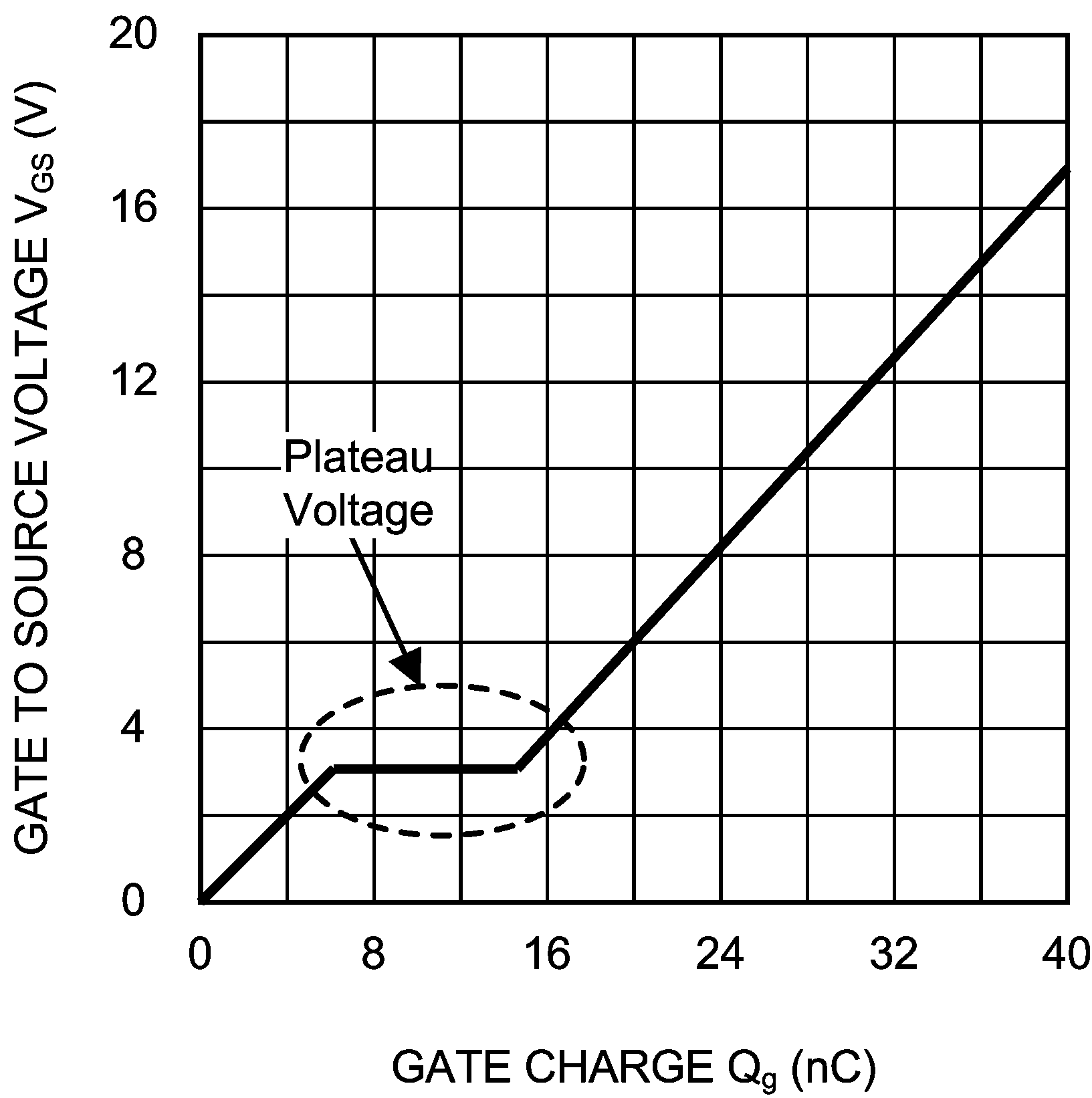 Figure 17. Typical MOSFET Gate Charge Curve
See following design example for estimated power dissipation calculation.
The main parameters for the input capacitor are the voltage rating, which must be greater than or equal to the maximum DC input voltage of the power supply, and its rms current rating. The maximum rms current is approximately 50% of the maximum load current.

where
When using low ESR ceramic capacitors on the input of the LM3150 controller, a resonant circuit can be formed with the impedance of the input power supply and parasitic impedance of long leads/PCB traces to the LM3150 input capacitors. TI recommends using a damping capacitor under these circumstances, such as aluminum electrolytic that will prevent ringing on the input. The damping capacitor should be chosen to be approximately five times greater than the parallel ceramic capacitors combination. The total input capacitance should be greater than 10 times the input inductance of the power supply leads/PCB trace. The damping capacitor should also be chosen to handle its share of the rms input current which is shared proportionately with the parallel impedance of the ceramic capacitors and aluminum electrolytic at the LM3150 switching frequency.
The CBYP capacitor should be placed directly at the VIN pin. The recommended value is 0.1 µF.

where
CVCC should be placed directly at the VCC pin with a recommended value of 1 µF to 4.7 µF. CBST creates a voltage used to drive the gate of the high-side FET. It is charged during the SW off-time. The recommended value for CBST is 0.47 µF. The EN bypass capacitor, CEN, recommended value is 1000 pF when driving the EN pin from open-drain type of signal.
8.2.3 Application Curves
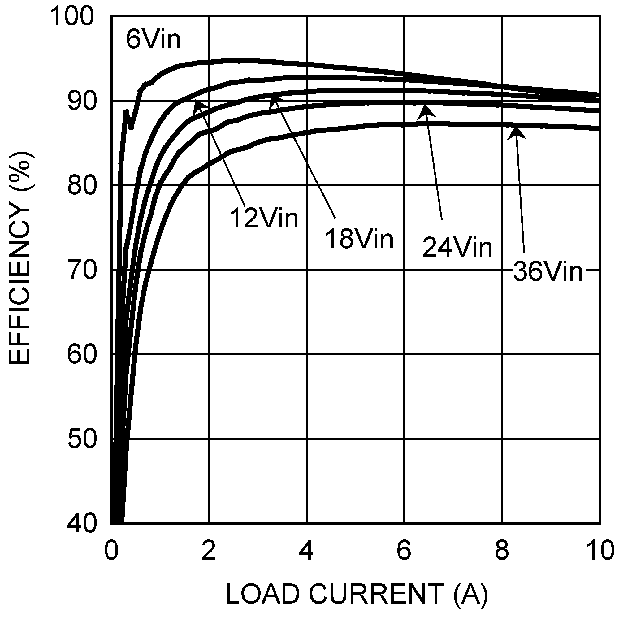 Figure 18. 250-kHz Efficiency vs Load
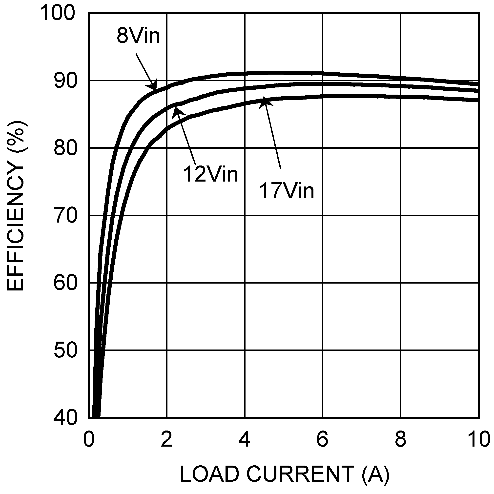 Figure 20. 750-kHz Efficiency vs Load
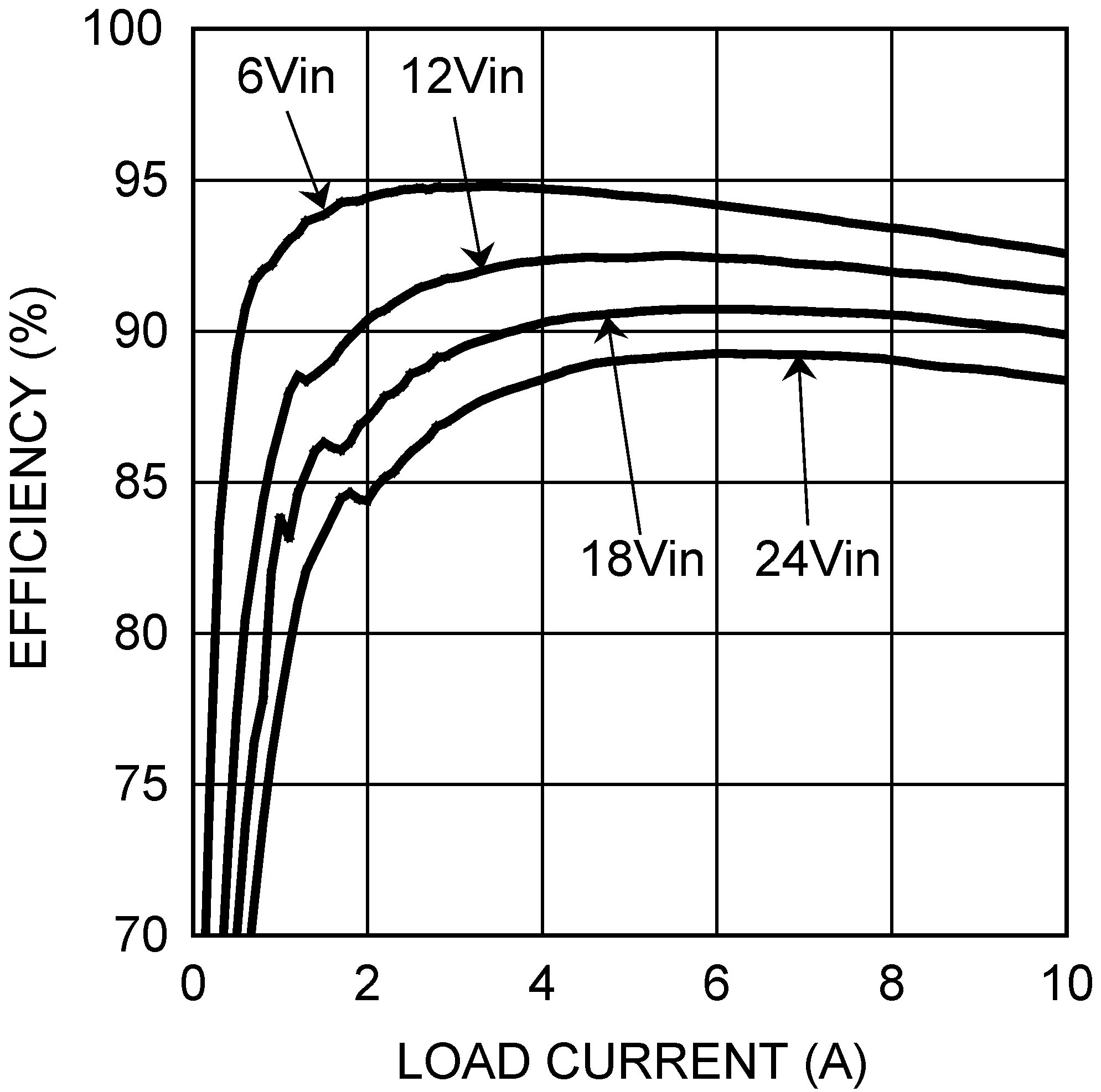 Figure 19. 500-kHz Efficiency vs Load