JAJSAC1G November 2007 – November 2023 LM3481
PRODUCTION DATA
- 1
- 1 特長
- 2 アプリケーション
- 3 概要
- 4 Pin Configuration and Functions
- 5 Specifications
- 6 Detailed Description
-
7 Application and Implementation
- 7.1 Application Information
- 7.2
Typical Applications
- 7.2.1
Boost Converter
- 7.2.1.1 Design Requirements
- 7.2.1.2
Detailed Design Procedure
- 7.2.1.2.1 Custom Design with WEBENCH Tools
- 7.2.1.2.2 Power Inductor Selection
- 7.2.1.2.3 Programming the Output Voltage and Output Current
- 7.2.1.2.4 Current Limit With Additional Slope Compensation
- 7.2.1.2.5 Power Diode Selection
- 7.2.1.2.6 Power MOSFET Selection
- 7.2.1.2.7 Input Capacitor Selection
- 7.2.1.2.8 Output Capacitor Selection
- 7.2.1.2.9 Driver Supply Capacitor Selection
- 7.2.1.2.10 Compensation
- 7.2.1.3 Application Curve
- 7.2.2 Typical SEPIC Converter
- 7.2.1
Boost Converter
- 7.3 Power Supply Recommendations
- 7.4 Layout
- 8 Device and Documentation Support
- 9 Revision History
- 10Mechanical, Packaging, and Orderable Information
6.3.5 Undervoltage Lockout (UVLO) Pin
The UVLO pin provides user programmable enable and shutdown thresholds. The UVLO pin is compared to an internal reference of 1.43 V (typical), and a resistor divider programs the enable threshold, VEN. When the IC is enabled, a 5-μA current is sourced out of the UVLO pin, which effectively causes a hysteresis, and the UVLO shutdown threshold, VSH, is now lower than the enable threshold. Setting these thresholds requires two resistors connected from the VIN pin to the UVLO pin and from the UVLO pin to GND (see Figure 6-12). Select the desired enable, VEN, and UVLO shutdown, VSH, threshold voltages and use the Equation 17 and Equation 18 to determine the resistance values:
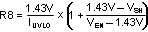
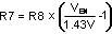
 Figure 6-12 UVLO Pin Resistor Divider
If the system is designed to work over wide input voltages, the voltage at the UVLO pin could exceed the voltage limit for the UVLO pin. In this case a zener diode can be connected between the UVLO pin and ground to prevent the UVLO voltage from rising above the maximum value.
If the UVLO pin function is not desired, select R8 and R7 of equal magnitude greater than 100 kΩ. This will allow VIN to be in control of the UVLO thresholds. The UVLO pin may also be used to implement the enable/disable function. If a signal pulls the UVLO pin below the 1.43 V (typical) threshold, the converter will be disabled.