JAJSAC1G November 2007 – November 2023 LM3481
PRODUCTION DATA
- 1
- 1 特長
- 2 アプリケーション
- 3 概要
- 4 Pin Configuration and Functions
- 5 Specifications
- 6 Detailed Description
-
7 Application and Implementation
- 7.1 Application Information
- 7.2
Typical Applications
- 7.2.1
Boost Converter
- 7.2.1.1 Design Requirements
- 7.2.1.2
Detailed Design Procedure
- 7.2.1.2.1 Custom Design with WEBENCH Tools
- 7.2.1.2.2 Power Inductor Selection
- 7.2.1.2.3 Programming the Output Voltage and Output Current
- 7.2.1.2.4 Current Limit With Additional Slope Compensation
- 7.2.1.2.5 Power Diode Selection
- 7.2.1.2.6 Power MOSFET Selection
- 7.2.1.2.7 Input Capacitor Selection
- 7.2.1.2.8 Output Capacitor Selection
- 7.2.1.2.9 Driver Supply Capacitor Selection
- 7.2.1.2.10 Compensation
- 7.2.1.3 Application Curve
- 7.2.2 Typical SEPIC Converter
- 7.2.1
Boost Converter
- 7.3 Power Supply Recommendations
- 7.4 Layout
- 8 Device and Documentation Support
- 9 Revision History
- 10Mechanical, Packaging, and Orderable Information
7.2.1.2.3 Programming the Output Voltage and Output Current
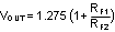
The output voltage can be programmed using a resistor divider between the output and the feedback pins, as shown in Figure 7-4. The resistors are selected such that the voltage at the feedback pin is 1.275 V. RF1 and RF2 can be selected using the equation,
A 100-pF capacitor may be connected between the feedback and ground pins to reduce noise.
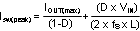
The maximum amount of current that can be delivered at the output can be controlled by the sense resistor, RSEN. Current limit occurs when the voltage that is generated across the sense resistor equals the current sense threshold voltage, VSENSE. Limits for VSENSE have been specified in the Electrical CharacteristicsElectrical CharacteristicsElectrical Characteristics section. This can be expressed as:
The peak current through the switch is equal to the peak inductor current.
Therefore for a boost converter,
Combining the two equations yields an expression for RSEN,
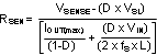
Evaluate RSEN at the maximum and minimum VIN values and choose the smallest RSEN calculated.
 Figure 7-4 Adjusting the Output Voltage