JAJSDC4
June 2017
LM385-1.2-MIL
PRODUCTION DATA.
1
特長
2
アプリケーション
3
概要
4
改訂履歴
5
Pin Configuration and Functions
6
Specifications
6.1
Absolute Maximum Ratings
6.2
ESD Ratings
6.3
Recommended Operating Conditions
6.4
Thermal Information
6.5
Electrical Characteristics
6.6
Typical Characteristics
7
Detailed Description
7.1
Overview
7.2
Functional Block Diagram
7.3
Feature Description
7.4
Device Functional Modes
8
Application and Implementation
8.1
Application Information
8.2
Typical Application
8.2.1
Design Requirements
8.2.2
Detailed Design Procedure
8.2.3
Application Curve
8.3
System Examples
8.3.1
Thermocouple Cold-Junction Compensator
8.3.2
Generating Reference Voltage with a Constant Current Source
9
Power Supply Recommendations
10
Layout
10.1
Layout Guidelines
10.2
Layout Example
11
デバイスおよびドキュメントのサポート
11.1
ドキュメントのサポート
11.1.1
関連資料
11.2
ドキュメントの更新通知を受け取る方法
11.3
コミュニティ・リソース
11.4
商標
11.5
静電気放電に関する注意事項
11.6
Glossary
12
メカニカル、パッケージ、および注文情報
パッケージ・オプション
メカニカル・データ(パッケージ|ピン)
YS|0
サーマルパッド・メカニカル・データ
発注情報
jajsdc4_oa
5
Pin Configuration and Functions
D, PS, PW or LP
8-Pin SOIC,SOP,TSSOP or TO-226
Top View
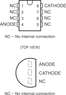
Pin Functions
PIN
TYPE
DESCRIPTION
NAME
LP
D, PS or PW
ANODE
1
4
I
Shunt Current/Voltage input
CATHODE
2
8
O
Common pin, normally connected to ground
NC
3
1, 2, 3, 5, 6, 7
—
No internal connection