SNVS555D January 2008 – December 2014 LM3881
PRODUCTION DATA.
- 1 Features
- 2 Applications
- 3 Description
- 4 Revision History
- 5 Pin Configuration and Functions
- 6 Specifications
- 7 Detailed Description
- 8 Application and Implementation
- 9 Power Supply Recommendations
- 10Layout
- 11Device and Documentation Support
- 12Mechanical, Packaging, and Orderable Information
7 Detailed Description
7.1 Overview
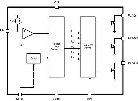
The LM3881 Simple Power Sequencer provides a simple solution for sequencing multiple rails in a controlled manner. An established clock signal facilitates control of the power up and power down of three open-drain FET output flags. These flags permit connection to shutdown or enable pins of linear regulators and/or switching regulators to control the operation of the power supplies. This allows design of a complete power system without the concern of large inrush currents or latch-up conditions that can occur during an uncontrolled startup. An invert (INV) pin reverses the logic of the output flags. This pin should be tied to a logic output high or low and not allowed to remain open circuit. The following discussion assumes the INV pin is held low such that the flag output is active high.
7.2 Functional Block Diagram
7.3 Feature Description
7.3.1 Adjustable Timing
A small external timing capacitor is connected to the TADJ pin that establishes the clock waveform. This capacitor is linearly charged/discharged by a fixed current source/sink, denoted ITADJ_SRC / ITADJ_SNK, of magnitude 12 µA between predefined voltage threshold levels, denoted VLTH and VHTH, to generate the timing waveform as shown in Figure 8.
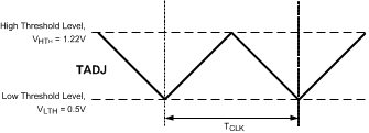 Figure 8. TADJ Pin Timing Waveform
Thus, the clock cycle duration is directly proportional to the timing capacitor value. Considering the TADJ voltage threshold levels and the charge/discharge current magnitude, it can be shown that the timing capacitor-clock period relationship is typically 120 µs/nF. For example, a 10-nF capacitor sets up a clock period of 1.2 ms.
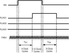
The timing sequence of the LM3881 is controlled by the enable (EN) pin. Upon power up, all the flags are held low until the precision enable pin exceeds its threshold. After the EN pin is asserted, the power-up sequence will commence and the open-drain flags will be sequentially released.
An internal counter will delay the first flag (FLAG1) from rising until a fixed time period, denoted by TD1 in Figure 9, elapses. This corresponds to at least nine, maximum 10, clock cycles depending on where EN is asserted relative to the clock signal. Upon release of the first flag, another timer will begin to delay the release of the second flag (FLAG2). This time delay, denoted TD2, corresponds to exactly eight clock periods. Similarly, FLAG3 is released after time delay TD3, again eight clock cycles, has expired. Accordingly, a TADJ capacitor of 10 nF generates typical time delays TD2 and TD3 of 9.6 ms and TD1 of from 10.8 ms to 12.0 ms.
The power-down sequence is the same as power up, but in reverse order. When the EN pin is deasserted, a timer will begin that delays the third flag (FLAG3) from pulling low. The second and first flag will then follow in a sequential manner after their appropriate time delays. These time delays, denoted TD4, TD5, TD6, are equal to TD1, TD2, TD3, respectively.
For robustness, the pulldown FET associated with each flag is designed such that it can sustain a short circuit to VCC.
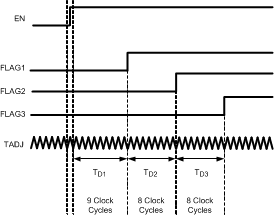 Figure 9. Power-Up Sequence, INV Low
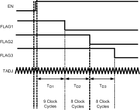 Figure 10. Power-Up Sequence, INV High
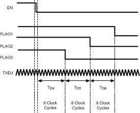 Figure 11. Power-Down Sequence, INV Low
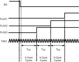 Figure 12. Power-Down Sequence, INV High
7.3.2 Enable Circuit
The enable circuit is designed with an internal comparator, referenced to a bandgap voltage (1.22 V), to provide a precision threshold. This allows the timing to be set externally using a capacitor as shown in Figure 13. Alternatively, sequencing can be based on a certain event such as a line voltage reaching 90% of its nominal value by employing a resistor divider from VCC to Enable.
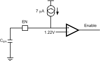 Figure 13. Precision Enable Circuit
Using the internal pullup current source to charge the external capacitor CEN, the time delay while the enable voltage reaches the required threshold, assuming EN is charging from 0V, can be calculated by the equation as follows.
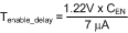
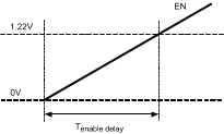 Figure 14. Enable Delay Timing
A resistor divider can also be used to enable the LM3881 based on exceeding a certain VCC supply voltage threshold. Take care when sizing the resistor divider to include the effects of the internal EN pullup current source. The supply voltage for which EN is asserted is given by
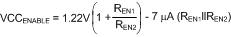
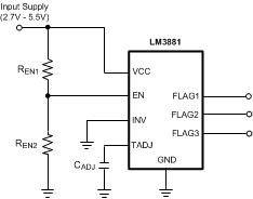 Figure 15. Enable Based On Input Supply Level
One of the features of the EN pin is that it provides glitch free operation. The timer will start counting at a rising threshold, but will always reset if the EN pin is deasserted before the first output flag is released. This is illustrated in Figure 16, assuming INV is low.
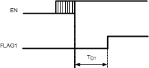 Figure 16. Enable Glitch Timing, INV Low
If the EN pin remains high for the entire power up sequence, then the part will operate as shown in the standard timing diagrams. However, if the EN signal is deasserted before the power-up sequence completes, the part will enter a controlled shutdown. This allows the system to initiate a controlled power sequence, preventing any latch conditions to occur. Figure 17 describes the flag sequence if the EN pin is deasserted after FLAG1 releases, but before the entire power-up sequence is completed. INV is assumed low.

7.4 Device Functional Modes
7.4.1 Power Up with EN Pin
The timing sequence of the Simple Power Sequencer is controlled entirely by the enable (EN) pin. Upon power up, all the flags are held low until this precision enable is pulled high. After the EN pin is asserted, the power-up sequence will commence.
7.4.2 Power Down with EN Pin
When EN pin is deasserted, the power down sequence will commence. A timer will begin that delays the third flag (FLAG3) from pulling low. The second and first flag will then follow in a sequential manner after their appropriate delays.
7.4.3 Noninverted Output Mode
When the INV pin is tied to a logic output low, the logic mode of the output flags is active high. This mode is useful to sequence power supplies which have an active high enable input.
7.4.4 Inverted Output Mode
When the INV pin is tied to a logic output high, the logic mode of the output flags is active low. This mode is useful to sequence power supplies which have an active low enable input.