SNVS555D January 2008 – December 2014 LM3881
PRODUCTION DATA.
- 1 Features
- 2 Applications
- 3 Description
- 4 Revision History
- 5 Pin Configuration and Functions
- 6 Specifications
- 7 Detailed Description
- 8 Application and Implementation
- 9 Power Supply Recommendations
- 10Layout
- 11Device and Documentation Support
- 12Mechanical, Packaging, and Orderable Information
5 Pin Configuration and Functions
VSSOP Package
8-Pin DGK
Top View
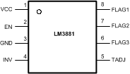
Pin Functions
| PIN | I/O | DESCRIPTION | |
|---|---|---|---|
| NAME | NO. | ||
| VCC | 1 | I | Input Supply |
| EN | 2 | I | Precision Enable |
| GND | 3 | – | Ground |
| INV | 4 | I | Output Logic Invert |
| TADJ | 5 | O | Timer Adjust |
| FLAG3 | 6 | O | Open-Drain Output 3 |
| FLAG2 | 7 | O | Open-Drain Output 2 |
| FLAG1 | 8 | O | Open-Drain Output 1 |