SNVS555D January 2008 – December 2014 LM3881
PRODUCTION DATA.
- 1 Features
- 2 Applications
- 3 Description
- 4 Revision History
- 5 Pin Configuration and Functions
- 6 Specifications
- 7 Detailed Description
- 8 Application and Implementation
- 9 Power Supply Recommendations
- 10Layout
- 11Device and Documentation Support
- 12Mechanical, Packaging, and Orderable Information
10 Layout
10.1 Layout Guidelines
- Pullup resistors should be connected between the flag output pins and a positive input supply, usually VCC. An independent flag supply may also be used. These resistors should be placed as close as possible to the Simple Power Sequencer and the flag supply. Minimal trace length is recommended to make the connections. A typical value for the pullup resistors is 100kΩ.
- For very tight sequencing requirements, minimal and equal trace lengths should be used to connect the flag outputs to the desired inputs. This will reduce any propagation delay and timing errors between the flag outputs along the line.
10.2 Layout Example
Figure 24 and Figure 25 are layout examples for the LM3881. These examples are taken from the LM3881EVAL. An optional component, assigned reference designator R4, is placed on the bottom side of the PCB to facilitate connection of INV to GND.
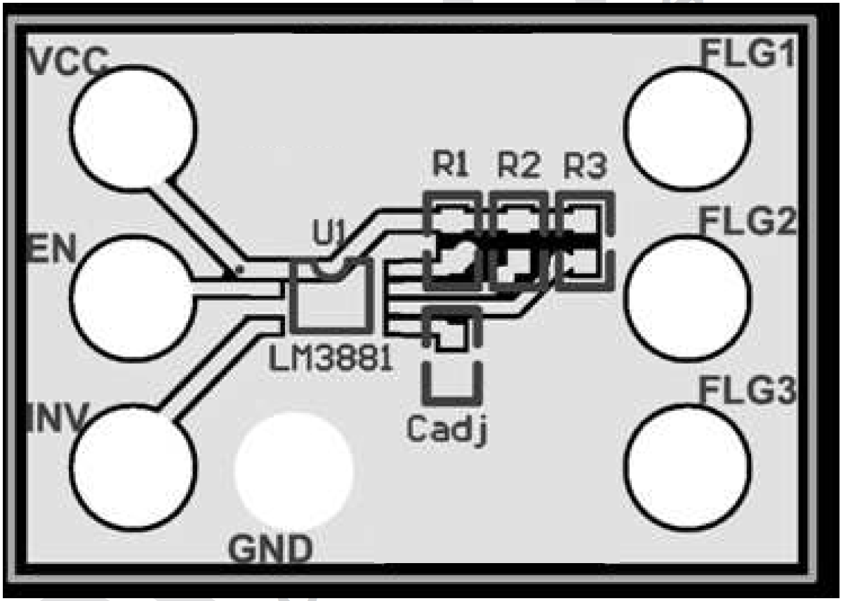 Figure 24. LM3881 Top
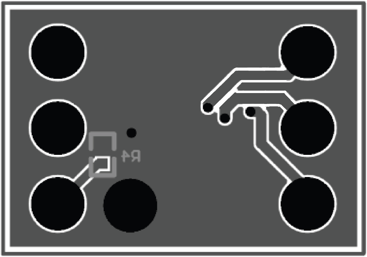 Figure 25. LM3881 Bottom