JAJSOR1D june 2022 – august 2023 LM5177
PRODUCTION DATA
- 1
- 1 特長
- 2 アプリケーション
- 3 概要
- 4 Revision History
- 5 Pin Configuration and Functions
- 6 Specifications
- 7 Parameter Measurement Information
-
8 Detailed Description
- 8.1 Overview
- 8.2 Functional Block Diagram
- 8.3
Feature Description
- 8.3.1 Power-On Reset (POR System)
- 8.3.2 Buck-Boost Control Scheme
- 8.3.3 Power Save Mode
- 8.3.4 Supply Voltage Selection – VMAX Switch
- 8.3.5 Enable and Undervoltage Lockout
- 8.3.6 Oscillator Frequency Selection
- 8.3.7 Frequency Synchronization
- 8.3.8 Voltage Regulation Loop
- 8.3.9 Output Voltage Tracking
- 8.3.10 Slope Compensation
- 8.3.11 Configurable Soft Start
- 8.3.12 Peak Current Sensor
- 8.3.13 Current Monitoring and Current Limit Control Loop
- 8.3.14 Short Circuit - Hiccup Protection
- 8.3.15 nFLT Pin and Protections
- 8.3.16 Device Configuration Pin
- 8.3.17 Dual Random Spread Spectrum – DRSS
- 8.3.18 Gate Driver
- 8.4 Device Functional Modes
-
9 Application and Implementation
- 9.1 Application Information
- 9.2
Typical Application
- 9.2.1 Design Requirements
- 9.2.2
Detailed Design Procedure
- 9.2.2.1 Custom Design with WEBENCH Tools
- 9.2.2.2 Frequency
- 9.2.2.3 Feedback Divider
- 9.2.2.4 Inductor and Current Sense Resistor Selection
- 9.2.2.5 Slope Compensation
- 9.2.2.6 Output Capacitor
- 9.2.2.7 Input Capacitor
- 9.2.2.8 UVLO Divider
- 9.2.2.9 Soft-Start Capacitor
- 9.2.2.10 MOSFETs QH1 and QL1
- 9.2.2.11 MOSFETs QH2 and QL2
- 9.2.2.12 Frequency Compensation
- 9.2.2.13 External Component Selection
- 9.2.3 Application Curves
- 9.3 System Examples
- 10Power Supply Recommendations
- 11Layout
- 12Device and Documentation Support
- 13Mechanical, Packaging, and Orderable Information
8.3.18 Gate Driver
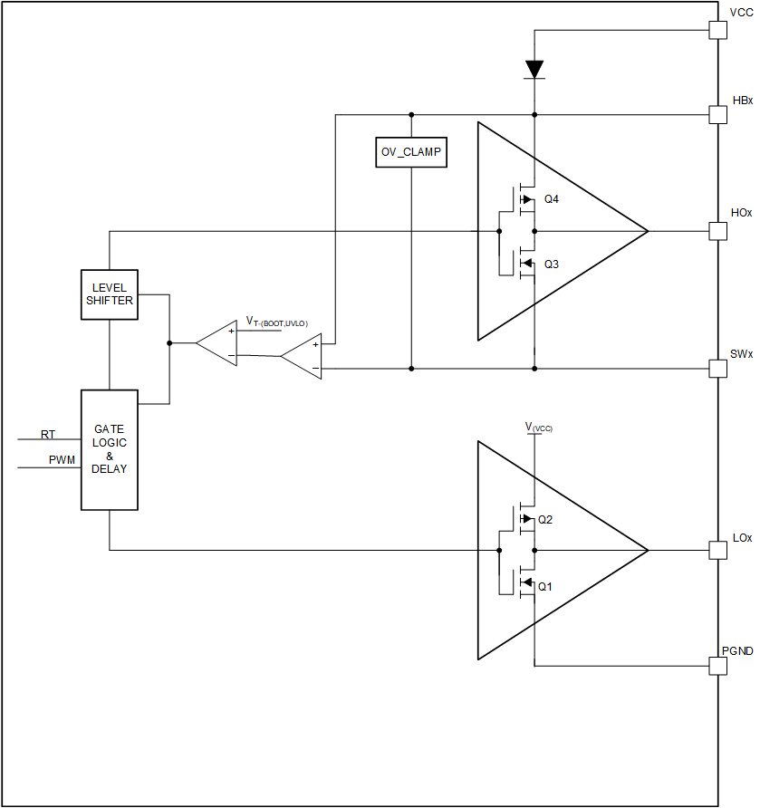
The LM5177 features four internal logic-level nMOS gate drivers. The drivers maintain the high frequency switching of both half bridges needed for a buck-boost operation. If the device is in boost or buck mode, the other half bridge high-side switch needs to be permanent on. The internal gate drivers support this by sharing the current from the other half bridge, which is switching. Therefore, a minimum of quiescent current can be assured as no additional char pump is needed. Due to the high drive current, it can support a wide range of external power FETs as well as a parallel operation of them.
The LO and HO outputs are protected with a shoot-through protection, which ensures that both outputs are not turned on at the same time. If the PWM modulation logic of the buck-boost turns the LOx pin off, the HOx pin is not turned on until the following are true:
- A minimum internal transition time (tt(dead)) is reached.
- The voltage on the LOx pin drops below the detection threshold VTH(GATEOUT).
The high-side supply voltage for the gate driver are monitored by an additional bootstrap UVLO comparator. This comparator monitors the differential voltage between SWx and HBx. If the voltage drops below the threshold the buck-boost converter operation turns off. The device restarts automatically once the positive going threshold is reached with the soft-start scheme.
Additionally, the LM5177 monitors the upper voltage between SWx and HBx. If this voltage exceeds the threshold voltage of the clamping circuit, it activates a internal current source to pull the voltage down.

Figure 8-21 Functional Block Diagram Gate Driver
External Gate Driver Support
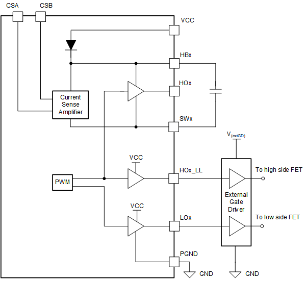
The LM5177 supports external gate driver by the HOx_LL pins. These pins provide the two high-side gate drive signals referenced to ground. By connecting the HOx_LL and LOx signals to a external gate driver the external power FETs can be controlled by the external gate driver. This feature for example is helpful in case no logic level FET is available and the application need to drive gate voltages higher the one the integrated gate drive supports.
The external bootstrap capacitors on HBx still needs to be placed in the schematic as the internal current sense amplifier is still supplied trough this pins. The HOx pin can be left floating. Make sure the supply voltage V(extGD) for each external gate driver maintains the necessary requirements for a 4-switch Buck-Boost such as 100% duty cycle and the isolation between each side of the full-bridge. Below Simplified Schematic External Gate Driver support show a functional block diagram of a possible connection for a external gate driver.
 Figure 8-22 Simplified Schematic External Gate Driver support