JAJSFG5D November 2008 – May 2018 LM7705
PRODUCTION DATA.
- 1 特長
- 2 アプリケーション
- 3 概要
- 4 改訂履歴
- 5 Pin Configuration and Functions
- 6 Specifications
- 7 Detailed Description
- 8 Application and Implementation
- 9 Power Supply Recommendations
- 10Layout
- 11デバイスおよびドキュメントのサポート
- 12メカニカル、パッケージ、および注文情報
8.2.3 Application Curves
The output voltage range of the LMP7701 has been measured, especially the range to ground level. A small DC signal, with a voltage swing of 50 mVPP is applied to the input. The digitized output voltage of the op amp is measured over a given time period, when its negative supply pin is connected to ground level or connected to the output of the LM7705.
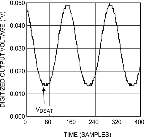
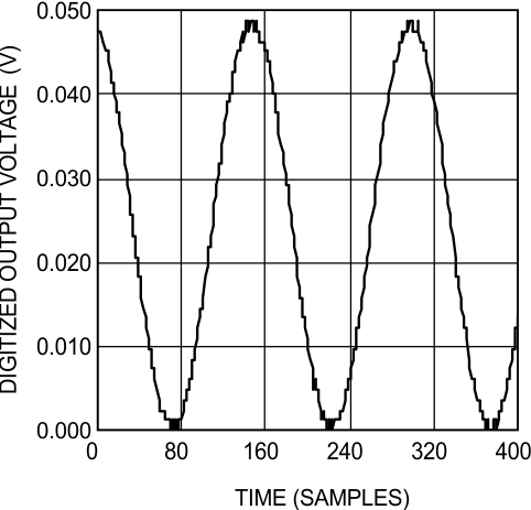
Figure 33 shows the digitized output voltage of the op amp when its negative supply pin is connected to ground level. The output of the amplifier saturates at a level of 14 mv (this is in line with the typical value of 18 mV given in the datasheet) The graph shows some fluctuations (1-bit quantization error). Figure 34 show the digitized output voltage of the op amp when its negative supply pin is connected to the output of the LM7705. Again, the graph shows some 1-bit quantization errors caused by the voltage ripple and output noise. In this case the op amps output level can reach the true zero output level.
Figure 33 and Figure 34 show that:
- With a single supply, the output of the amplifier is limited by the VDSAT of the output stage.
- The amplifier can be used as a true zero output using a LM7705.
- The quantization error of the digitized output voltage is caused by the noise and the voltage ripple.
- Using the LM7705 does not increase the quantization error in this set up.
 Figure 33. Digitized Output Voltage Without LM7705
  Figure 34. Digitized Output Voltage With LM7705