JAJSFG5D November   2008  – May 2018 LM7705

PRODUCTION DATA.  

  1. 特長
  2. アプリケーション
  3. 概要
    1.     Device Images
      1.      代表的なアプリケーション
  4. 改訂履歴
  5. Pin Configuration and Functions
    1.     Pin Functions
  6. Specifications
    1. 6.1 Absolute Maximum Ratings
    2. 6.2 ESD Ratings
    3. 6.3 Recommended Operating Conditions
    4. 6.4 Thermal Information
    5. 6.5 3.3-V Electrical Characteristics
    6. 6.6 5-V Electrical Characteristics
    7. 6.7 Typical Characteristics
  7. Detailed Description
    1. 7.1 Overview
    2. 7.2 Functional Block Diagram
    3. 7.3 Feature Description
      1. 7.3.1 Supply Voltage
      2. 7.3.2 Output Voltage and Line Regulation
      3. 7.3.3 Output Current and Load Regulation
      4. 7.3.4 Quiescent Current
    4. 7.4 Device Functional Modes
      1. 7.4.1 General Amplifier Application
        1. 7.4.1.1 One-Stage, Single-Supply True Zero Amplifier
        2. 7.4.1.2 Two-Stage, Single-Supply True Zero Amplifier
        3. 7.4.1.3 Dual-Supply, True Zero Amplifiers
  8. Application and Implementation
    1. 8.1 Application Information
      1. 8.1.1 Functional Description
      2. 8.1.2 Technical Description
      3. 8.1.3 Charge Pump Theory
    2. 8.2 Typical Application
      1. 8.2.1 Design Requirements
      2. 8.2.2 Detailed Design Procedure
        1. 8.2.2.1 Basic Setup
      3. 8.2.3 Application Curves
  9. Power Supply Recommendations
  10. 10Layout
    1. 10.1 Layout Guidelines
    2. 10.2 Layout Examples
  11. 11デバイスおよびドキュメントのサポート
    1. 11.1 コミュニティ・リソース
    2. 11.2 商標
    3. 11.3 静電気放電に関する注意事項
    4. 11.4 Glossary
  12. 12メカニカル、パッケージ、および注文情報

パッケージ・オプション

メカニカル・データ(パッケージ|ピン)
サーマルパッド・メカニカル・データ
発注情報

Pin Configuration and Functions

DGK Package
8-Pin VSSOP
Top View
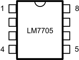
LM7705 20173002.gif

Pin Functions

PIN TYPE DESCRIPTION
NAME NO.
CF+ 1 Analog CFLY Positive Capacitor Connection
VSS 2 Ground Power Ground
SD 3 Input Shutdown Pin
If SD pin is LOW, device is ON
If SD pin is HIGH, device is OFF
VDD 4 Power Positive Supply Voltage
VSS 5 Ground Power Ground
VOUT 6 Output Output Voltage
CRES 7 Analog Reserve Capacitor Connection
CF- 8 Analog CFLY Negative Capacitor Connection