JAJSDD7 June 2017 LMC6482-MIL
PRODUCTION DATA.
- 1 特長
- 2 アプリケーション
- 3 概要
- 4 改訂履歴
- 5 Pin Configuration and Functions
- 6 Specifications
- 7 Detailed Description
- 8 Application and Implementation
- 9 Power Supply Recommendations
- 10Layout
- 11デバイスおよびドキュメントのサポート
- 12メカニカル、パッケージ、および注文情報
6 Specifications
6.1 Absolute Maximum Ratings
over operating free-air temperature range (unless otherwise noted)(1)(2)| MIN | MAX | UNIT | ||
|---|---|---|---|---|
| Differential Input Voltage | ±Supply Voltage | |||
| Voltage at Input/Output Pin | (V−) −0.3 | (V+) +0.3 | V | |
| Supply Voltage (V+ − V−) | 16 | V | ||
| Current at Input Pin (3) | −5 | 5 | mA | |
| Current at Output Pin (4) (5) | −30 | 30 | mA | |
| Current at Power Supply Pin | 40 | mA | ||
| Lead Temperature (Soldering, 10 sec.) | 260 | °C | ||
| Junction Temperature (6) | 150 | °C | ||
| Storage temperature, Tstg | −65 | 150 | °C | |
(1) Stresses beyond those listed under Absolute Maximum Ratings may cause permanent damage to the device. These are stress ratings only, which do not imply functional operation of the device at these or any other conditions beyond those indicated under Recommended Operating Conditions. Exposure to absolute-maximum-rated conditions for extended periods may affect device reliability.
(2) If Military/Aerospace specified devices are required, please contact the TI Sales Office/Distributors for availability and specifications.
(3) Limiting input pin current is only necessary for input voltages that exceed absolute maximum input voltage ratings.
(4) Applies to both single-supply and split-supply operation. Continuous short circuit operation at elevated ambient temperature can result in exceeding the maximum allowed junction temperature of 150°C. Output currents in excess of ±30 mA over long term may adversely affect reliability.
(5) Do not short circuit output to V+, when V+ is greater than 13 V or reliability will be adversely affected.
(6) The maximum power dissipation is a function of TJ(max), RθJA, and TA. The maximum allowable power dissipation at any ambient temperature is PD = (TJ(max) − TA)/θJA. All numbers apply for packages soldered directly into a PC board.
6.2 ESD Ratings
| VALUE | UNIT | |||
|---|---|---|---|---|
| V(ESD) | Electrostatic discharge | Human-body model (HBM), per ANSI/ESDA/JEDEC JS-001(1) | ±1500 | V |
(1) JEDEC document JEP155 states that 500-V HBM allows safe manufacturing with a standard ESD control process.
6.3 Recommended Operating Conditions
over operating free-air temperature range (unless otherwise noted)(1)| MIN | MAX | UNIT | ||
|---|---|---|---|---|
| Supply Voltage | 3 | 15.5 | V | |
| Junction Temperature Range | LMC6482M | –55 | 125 | °C |
(1) Stresses beyond those listed under Absolute Maximum Ratings may cause permanent damage to the device. These are stress ratings only, which do not imply functional operation of the device at these or any other conditions beyond those indicated under Recommended Operating Conditions. Exposure to absolute-maximum-rated conditions for extended periods may affect device reliability.
6.4 Thermal Information
| THERMAL METRIC(1) | LMC6482-MIL | LMC6482-MIL | LMC6482-MIL | UNIT | |
|---|---|---|---|---|---|
| D (SOIC) | DGK (VSSOP) | P (PDIP) | |||
| 8 PINS | 8 PINS | 8 PINS | |||
| RθJA | Junction-to-ambient thermal resistance | 155 | 194 | 90 | °C/W |
(1) For more information about traditional and new thermal metrics, see the IC Package Thermal Metrics application report, SPRA953.
6.5 Electrical Characteristics for V+ = 5 V
Unless otherwise specified, all limits specified for TJ = 25°C, V+ = 5 V, V− = 0 V, VCM = VO = V+/2 and RL > 1 M.| PARAMETER | TEST CONDITIONS | TJ = 25°C | At Temperature Extremes(7) | UNIT | ||||||
|---|---|---|---|---|---|---|---|---|---|---|
| MIN | TYP(1) | MAX(2) | MIN | TYP(1) | MAX(2) | |||||
| DC Electrical Characteristics | ||||||||||
| VOS | Input Offset Voltage | 0.11 | 3 | 3.8 | mV | |||||
| TCVOS | Input Offset Voltage Average Drift | 1 | μV/°C | |||||||
| IB | Input Current | See (3) | 0.02 | 10 | pA | |||||
| IOS | Input Offset Current | See (3) | 0.01 | 5 | pA | |||||
| CIN | Common-Mode Input Capacitance | 3 | pF | |||||||
| RIN | Input Resistance | 10 | TeraΩ | |||||||
| CMRR | Common-Mode Rejection Ratio | 0 V ≤ VCM ≤ 15 V V+ = 15 V |
65 | 82 | 60 | dB | ||||
| 0 V ≤ VCM ≤ 5 V V+ = 5 V |
65 | 82 | 60 | |||||||
| +PSRR | Positive Power Supply Rejection Ratio | 5 V ≤ V+ ≤ 15 V, V− = 0 V VO = 2.5 V |
65 | 82 | 60 | dB | ||||
| −PSRR | Negative Power Supply Rejection Ratio | −5 V ≤ V− ≤ −15 V, V+ = 0 V VO = −2.5 V |
65 | 82 | 60 | dB | ||||
| VCM | Input Common-Mode Voltage Range | V+ = 5 V and 15 V For CMRR ≥ 50 dB |
V− − 0.3 | −0.25 | 0 | V | ||||
| V+ + 0.25 | V+ + 0.3 | V+ | ||||||||
| AV | Large Signal Voltage Gain | RL = 2 kΩ(4)(3) | Sourcing | 120 | 666 | 60 | V/mV | |||
| Sinking | 35 | 75 | 18 | |||||||
| RL = 600 Ω(4)(3) | Sourcing | 50 | 300 | 25 | ||||||
| Sinking | 15 | 35 | 8 | |||||||
| VO | Output Swing | V+ = 5 V RL = 2 kΩ to V+/2 |
4.8 | 4.9 | 4.7 | V | ||||
| 0.1 | 0.18 | 0.24 | ||||||||
| V+ = 5 V RL = 600 Ω to V+/2 |
4.5 | 4.7 | 4.24 | V | ||||||
| 0.3 | 0.5 | 0.65 | ||||||||
| V+ = 15 V RL = 2k Ω to V+/2 |
14.4 | 14.7 | 14.2 | V | ||||||
| 0.16 | 0.32 | 0.45 | ||||||||
| V+ = 15 V RL = 600 Ω to V+/2 |
13.4 | 14.1 | 13 | V | ||||||
| 0.5 | 1 | 1.3 | ||||||||
| ISC | Output Short Circuit Current V+ = 5 V |
Sourcing, VO = 0 V | 16 | 20 | 10 | mA | ||||
| Sinking, VO = 5 V | 11 | 15 | 8 | |||||||
| ISC | Output Short Circuit Current V+ = 15 V |
Sourcing, VO = 0 V | 28 | 30 | 20 | mA | ||||
| Sinking, VO = 12 V(5) |
30 | 30 | 22 | |||||||
| IS | Supply Current | Both Amplifiers V+ = +5 V, VO = V+/2 |
1 | 1.4 | 1.9 | mA | ||||
| Both Amplifiers V+ = 15 V, VO = V+/2 |
1.3 | 1.6 | 2 | |||||||
| AC Electrical Characteristics | ||||||||||
| SR | Slew Rate | See (6) | 0.9 | 1.3 | 0.54 | V/μs | ||||
| GBW | Gain-Bandwidth Product | V+ = 15 V | 1.5 | MHz | ||||||
| φm | Phase Margin | 50 | Deg | |||||||
| Gm | Gain Margin | 15 | dB | |||||||
| Amp-to-Amp Isolation | See (5) | 150 | dB | |||||||
| en | Input-Referred Voltage Noise | F = 1 kHz Vcm = 1 V |
37 | nV/√Hz | ||||||
| In | Input-Referred Current Noise | F = 1 kHz | 0.03 | pA/√Hz | ||||||
| T.H.D. | Total Harmonic Distortion | F = 10 kHz, AV = −2 RL = 10 kΩ, VO = 4.1 VPP |
0.01% | |||||||
| F = 10 kHz, AV = −2 RL = 10 kΩ, VO = 8.5 VPP V+ = 10 V |
0.01% | |||||||||
(1) Typical Values represent the most likely parametric norm.
(2) All limits are specified by testing or statistical analysis.
(3) Ensured limits are dictated by tester limitations and not device performance. Actual performance is reflected in the typical value.
(4) V+ = 15 V, VCM = 7.5 V and RL connected to 7.5 V. For Sourcing tests, 7.5 V ≤ VO ≤ 11.5 V. For Sinking tests, 3.5 V ≤ VO ≤ 7.5 V.
(5) Input referred, V+ = 15 V and RL = 100 kΩ connected to 7.5 V. Each amp excited in turn with 1 kHz to produce VO = 12 VPP.
(6) V + = 15V. Connected as Voltage Follower with 10V step input. Number specified is the slower of either the positive or negative slew rates.
(7) See Recommended Operating Conditions for operating temperature ranges.
6.6 Electrical Characteristics for V+ = 3 V
Unless otherwise specified, all limits specified for TJ = 25°C, V+ = 3V, V− = 0V, VCM = VO = V+/2 and RL > 1M.| PARAMETER | TEST CONDITIONS | TJ = 25°C | At Temperature Extremes(4) | UNIT | |||||||
|---|---|---|---|---|---|---|---|---|---|---|---|
| MIN | TYP(1) | MAX(2) | MIN | TYP(1) | MAX(2) | ||||||
| DC Electrical Characteristics | |||||||||||
| VOS | Input Offset Voltage | 0.9 | 3 | 3.8 | mV | ||||||
| TCVOS | Input Offset Voltage Average Drift | 2 | μV/°C | ||||||||
| IB | Input Bias Current | 0.02 | pA | ||||||||
| IOS | Input Offset Current | 0.01 | pA | ||||||||
| CMRR | Common Mode Rejection Ratio | 0 V ≤ VCM ≤ 3 V | 60 | 74 | dB | ||||||
| PSRR | Power Supply Rejection Ratio | 3 V ≤ V+ ≤ 15 V, V− = 0 V | 60 | 80 | dB | ||||||
| VCM | Input Common-Mode Voltage Range | For CMRR ≥ 50 dB | V− −0.25 | 0 | V | ||||||
| V+ | V+ + 0.25 | V | |||||||||
| VO | Output Swing | RL = 2 kΩ to V+/2 | 2.8 | V | |||||||
| 0.2 | V | ||||||||||
| RL = 600 Ω to V+/2 | 2.5 | 2.7 | V | ||||||||
| 0.37 | 0.6 | V | |||||||||
| IS | Supply Current | Both Amplifiers | 0.825 | 1.2 | 1.6 | mA | |||||
| AC Electrical Characteristics | |||||||||||
| SR | Slew Rate | See (3) | 0.9 | V/μs | |||||||
| GBW | Gain-Bandwidth Product | 1 | MHz | ||||||||
| T.H.D. | Total Harmonic Distortion | F = 10 kHz, AV = −2 RL = 10 kΩ, VO = 2 VPP |
0.01% | ||||||||
(1) Typical Values represent the most likely parametric norm.
(2) All limits are specified by testing or statistical analysis.
(3) Connected as voltage Follower with 2-V step input. Number specified is the slower of either the positive or negative slew rates.
(4) See Recommended Operating Conditions for operating temperature ranges.
6.7 Typical Characteristics
VS = 15 V, Single Supply, TA = 25°C unless otherwise specified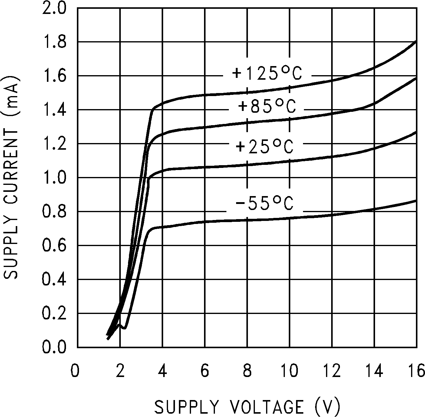 Figure 1. Supply Current vs. Supply Voltage
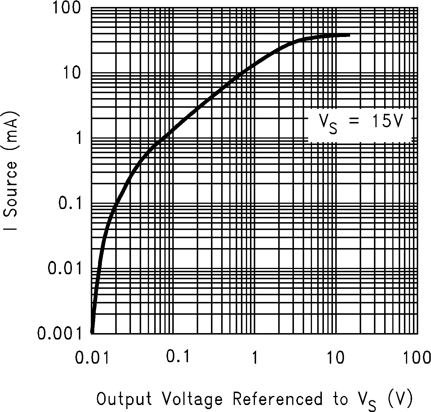 Figure 3. Sourcing Current vs. Output Voltage
 Figure 5. Sourcing Current vs. Output Voltage
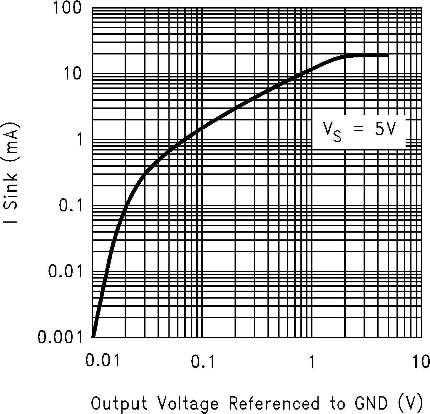 Figure 7. Sinking Current vs. Output Voltage
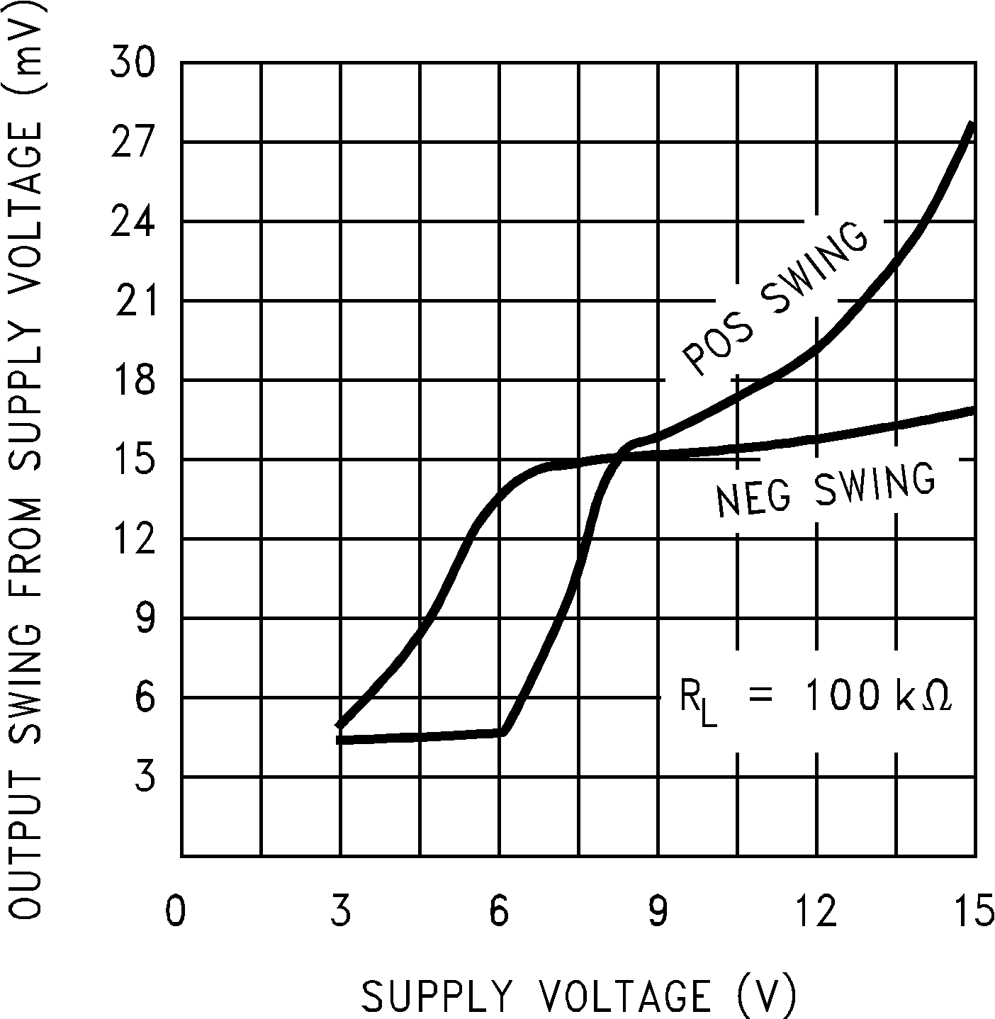 Figure 9. Output Voltage Swing vs. Supply Voltage
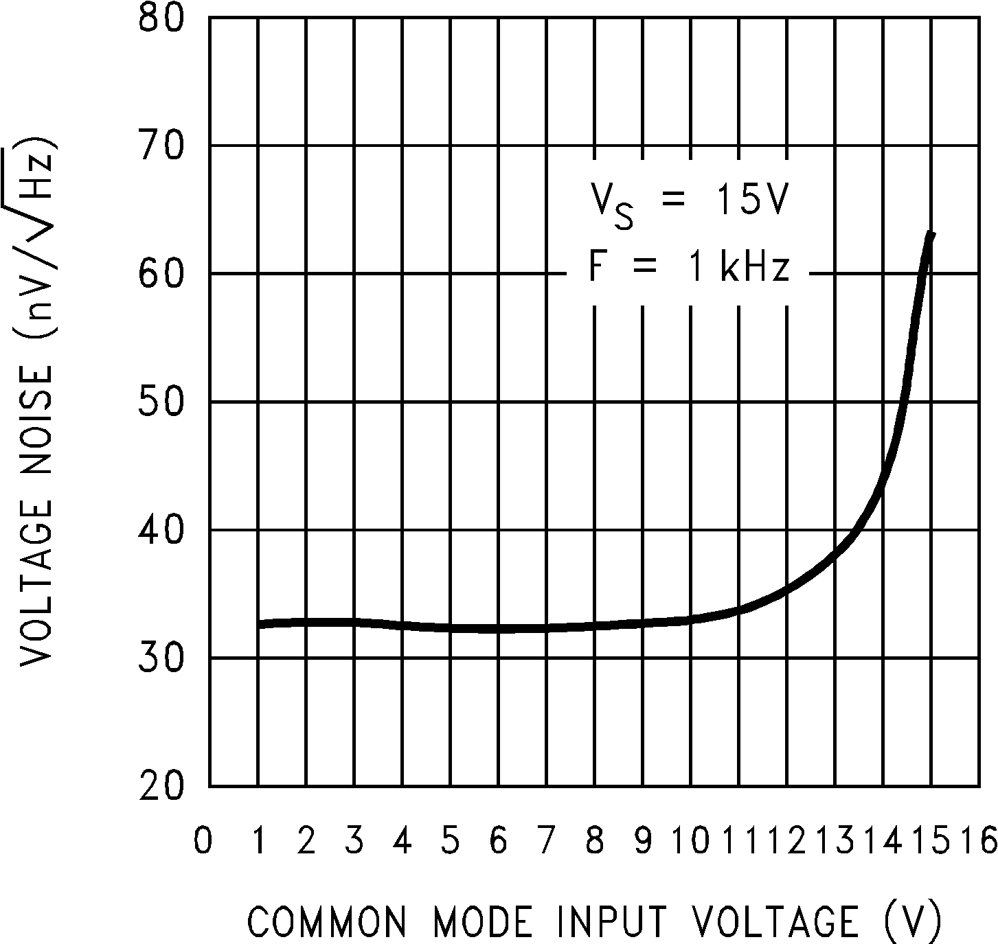 Figure 11. Input Voltage Noise vs. Input Voltage
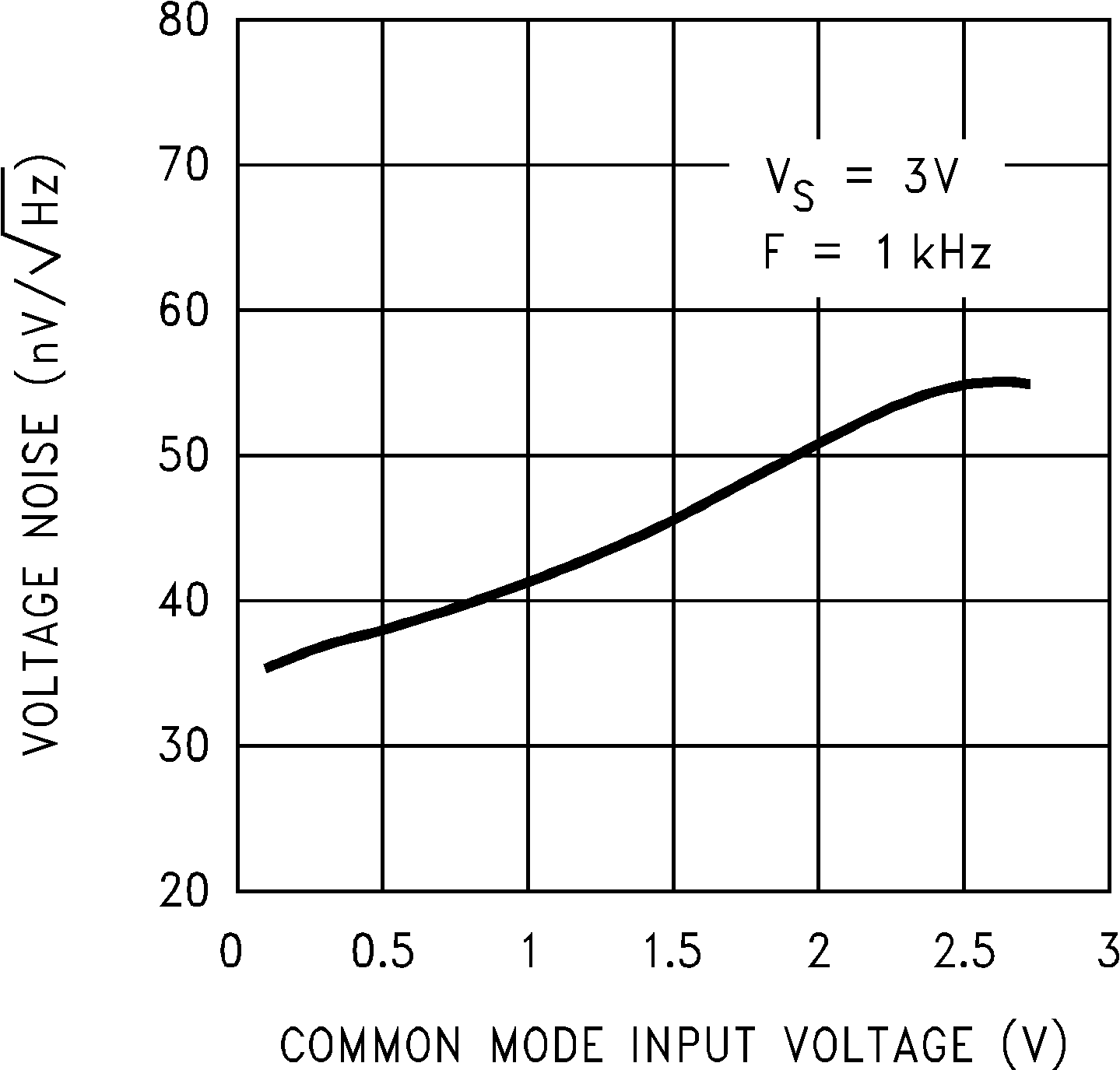 Figure 13. Input Voltage Noise vs. Input Voltage
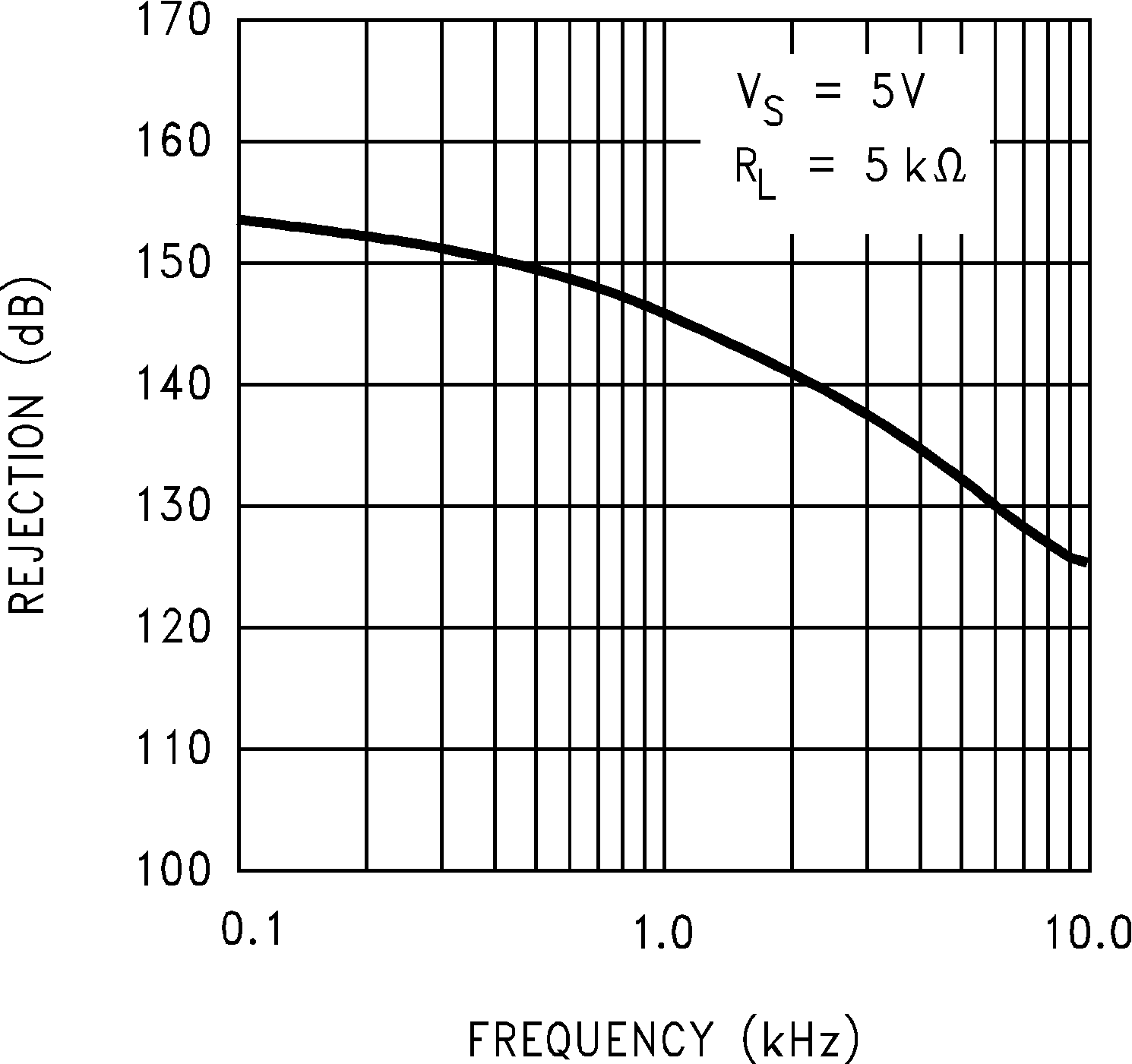 Figure 15. Crosstalk Rejection vs. Frequency
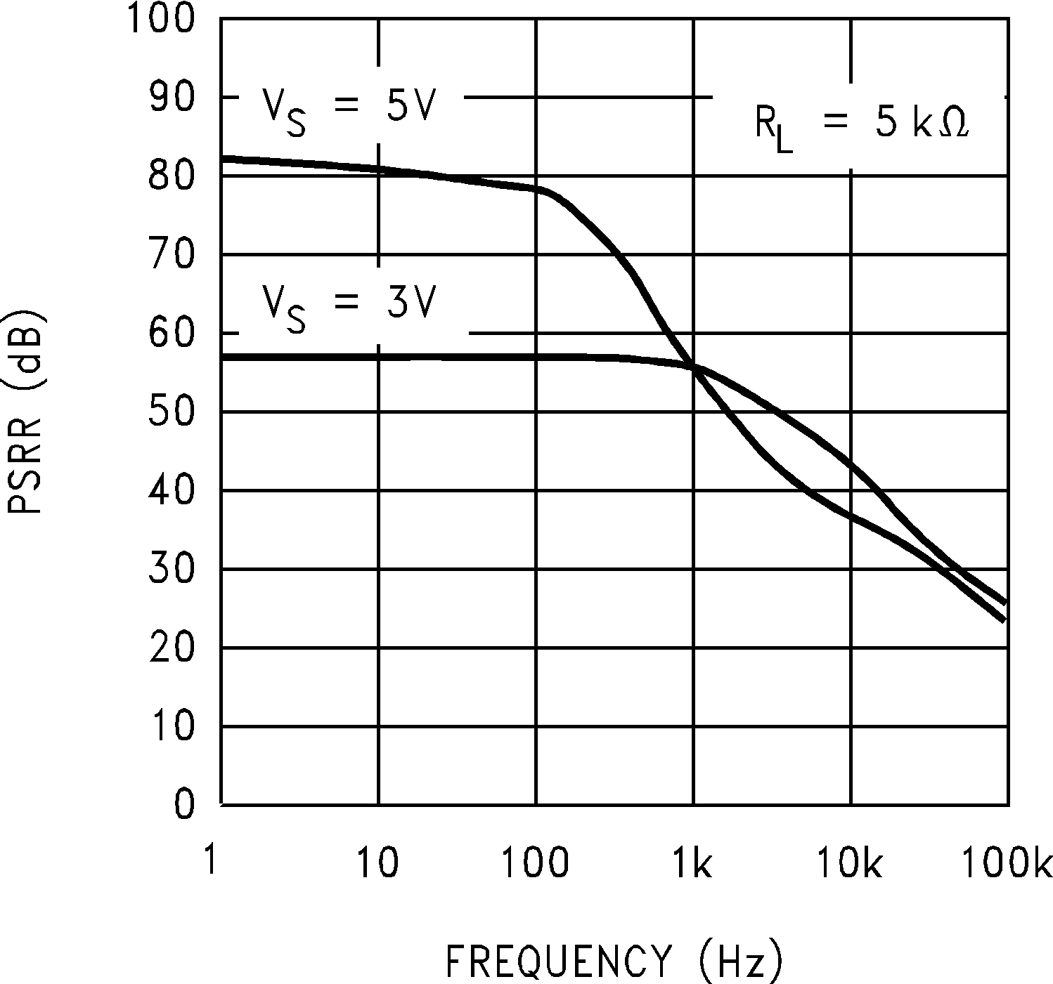 Figure 17. Negative PSRR vs. Frequency
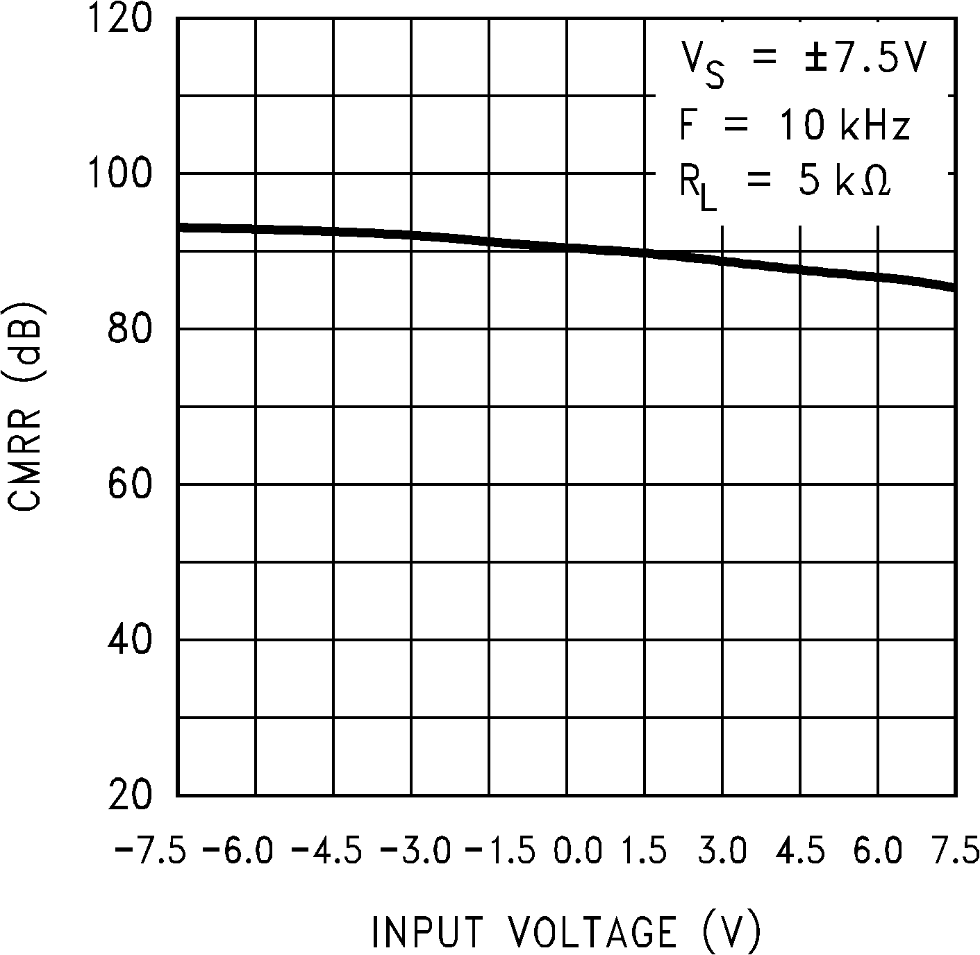 Figure 19. CMRR vs. Input Voltage
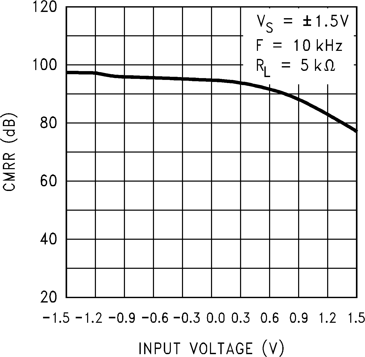 Figure 21. CMRR vs. Input Voltage
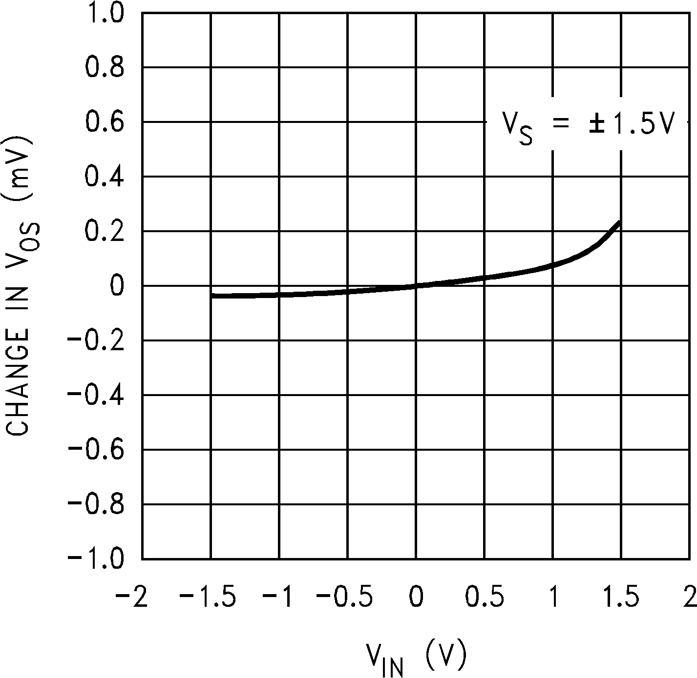 Figure 23. ΔvOS vs. CMR
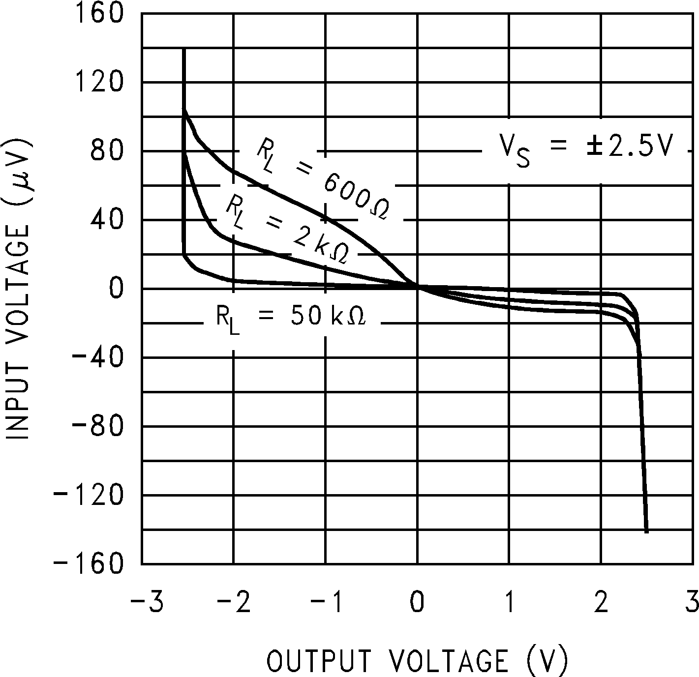 Figure 25. Input Voltage vs. Output Voltage
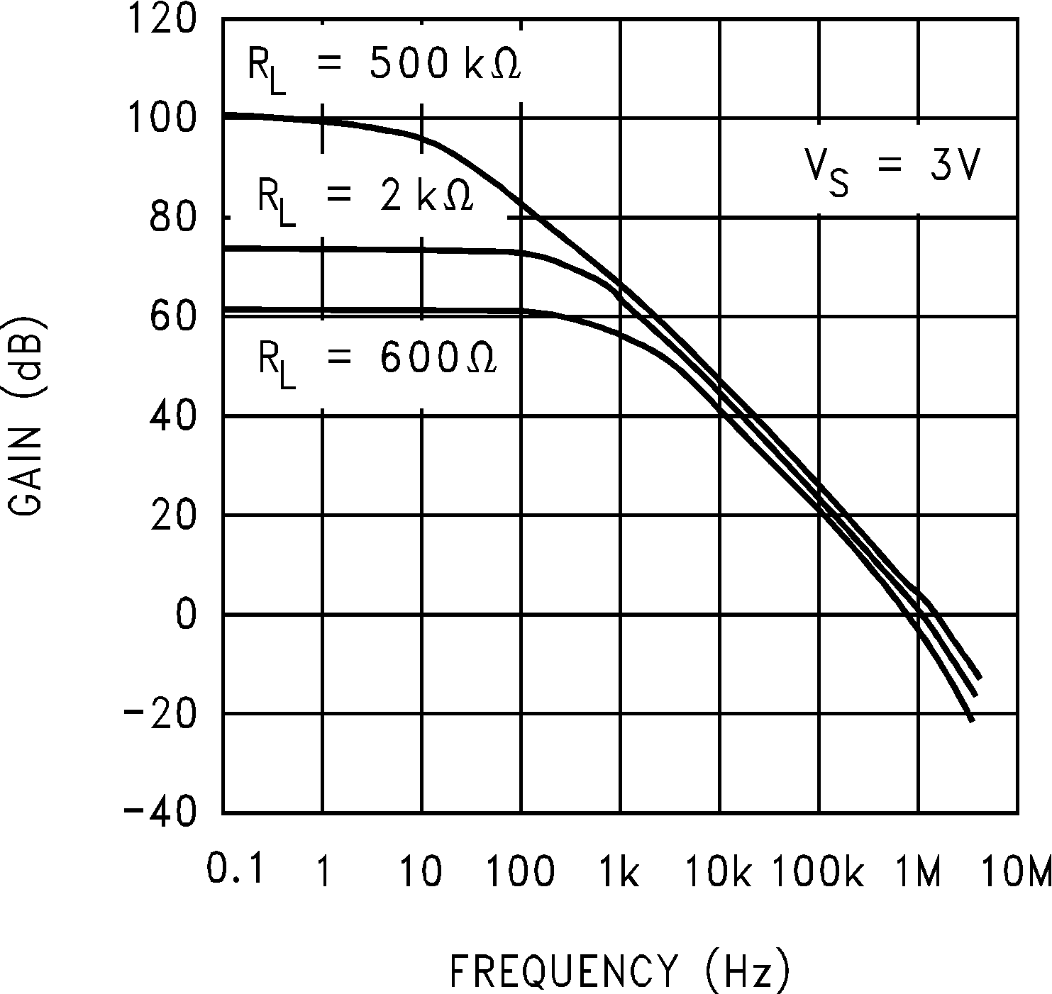 Figure 27. Open-Loop Frequency Response
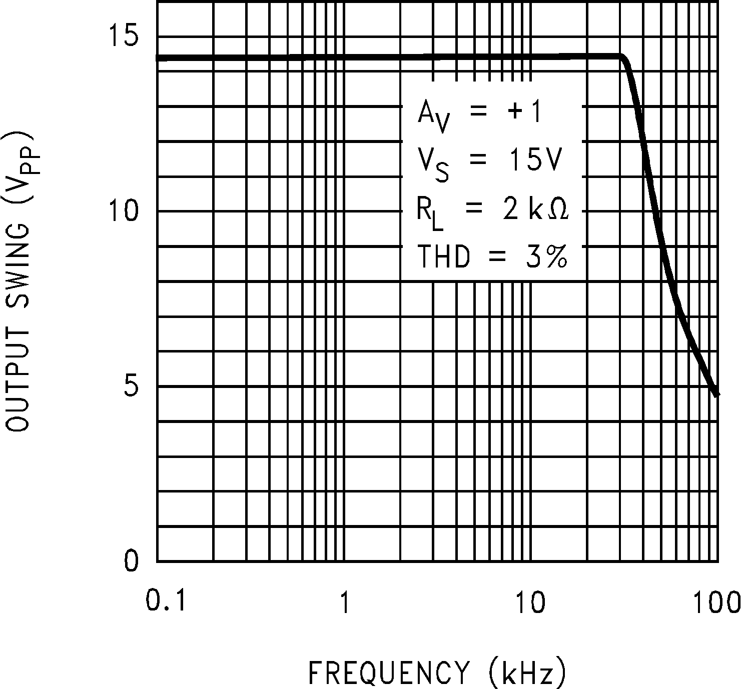 Figure 29. Maximum Output Swing vs. Frequency
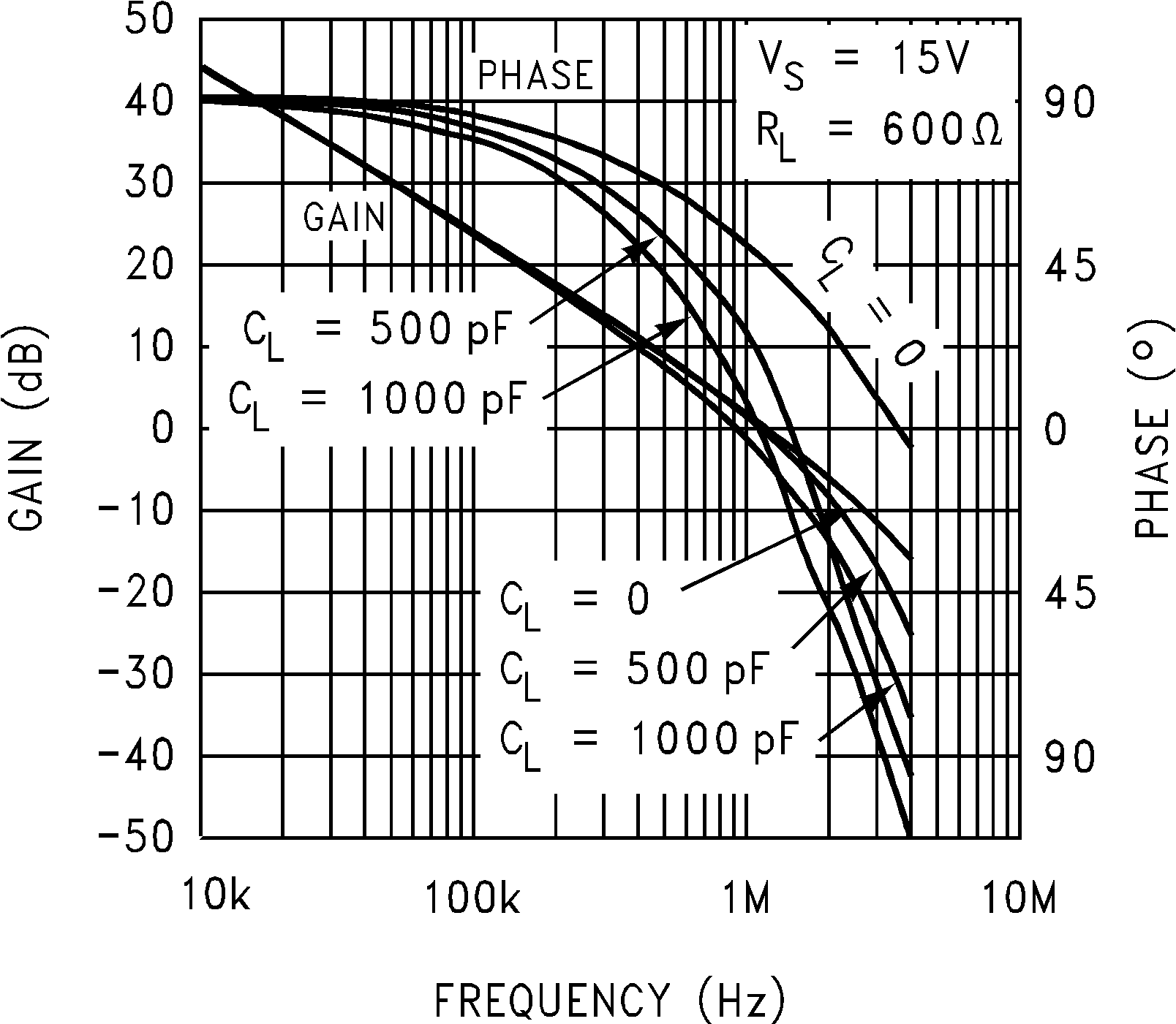 Figure 31. Gain and Phase vs. Capacitive Load
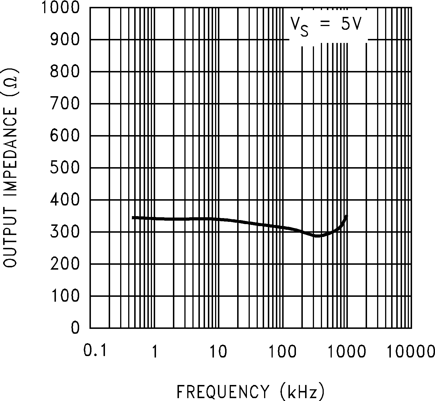 Figure 33. Open-Loop Output Impedance vs. Frequency
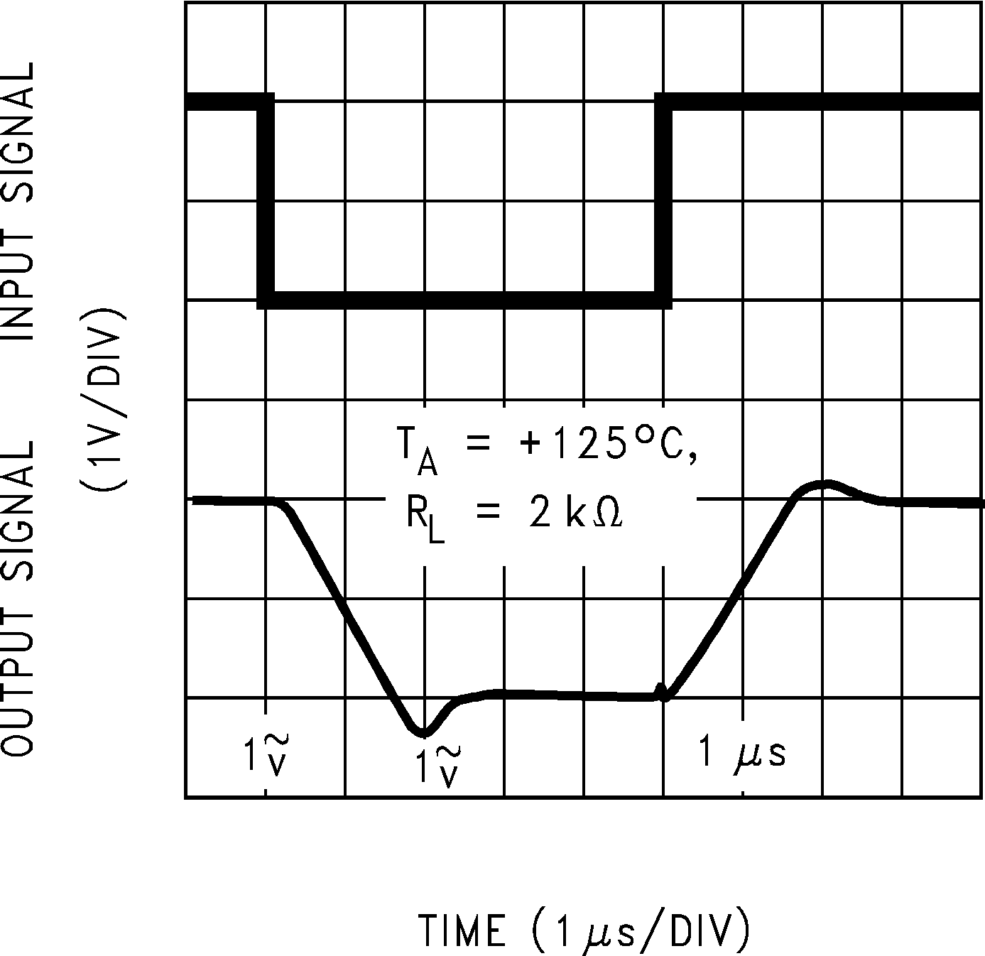 Figure 35. Noninverting Large Signal Pulse Response
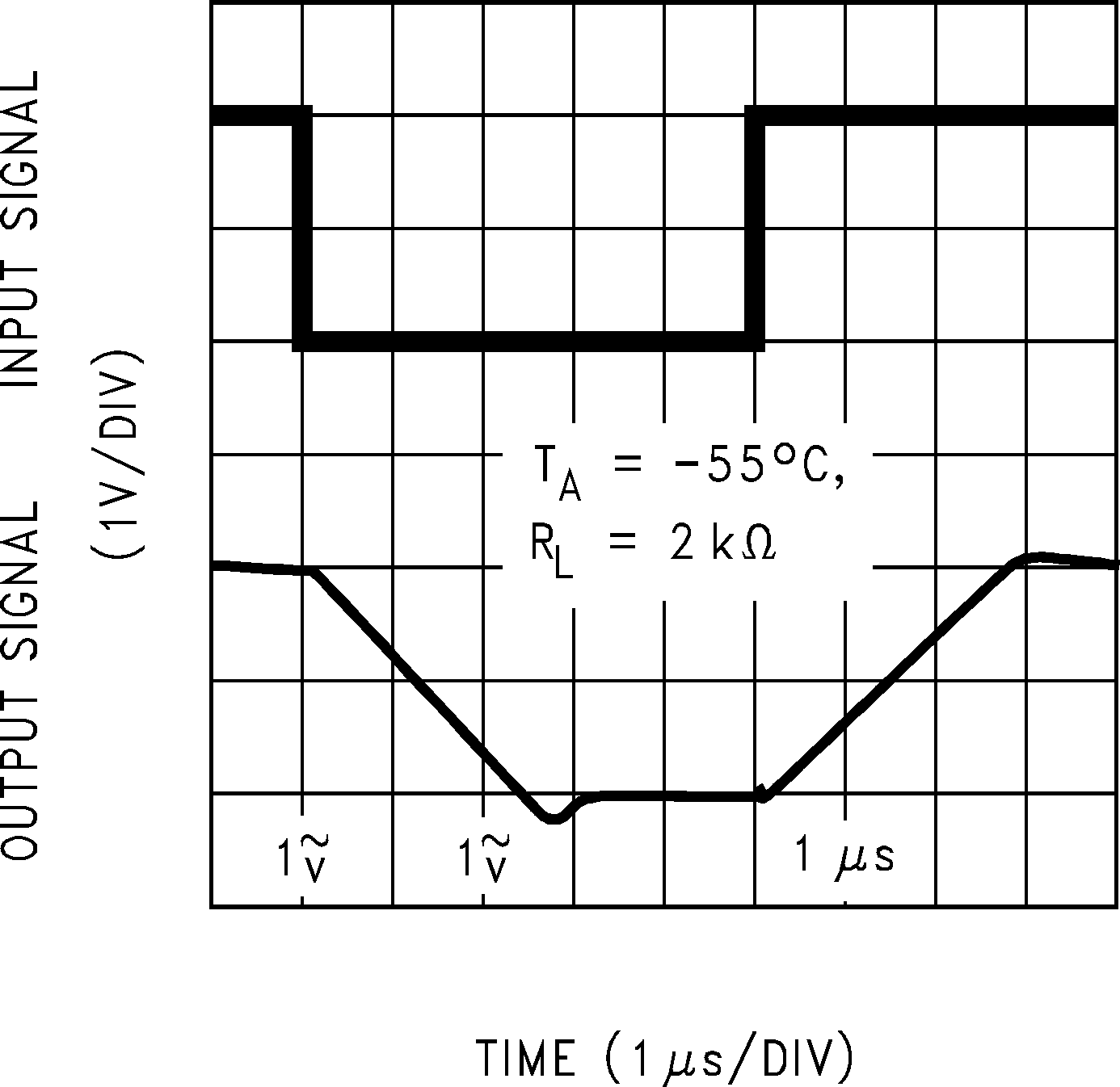 Figure 37. Noninverting Large Signal Pulse Response
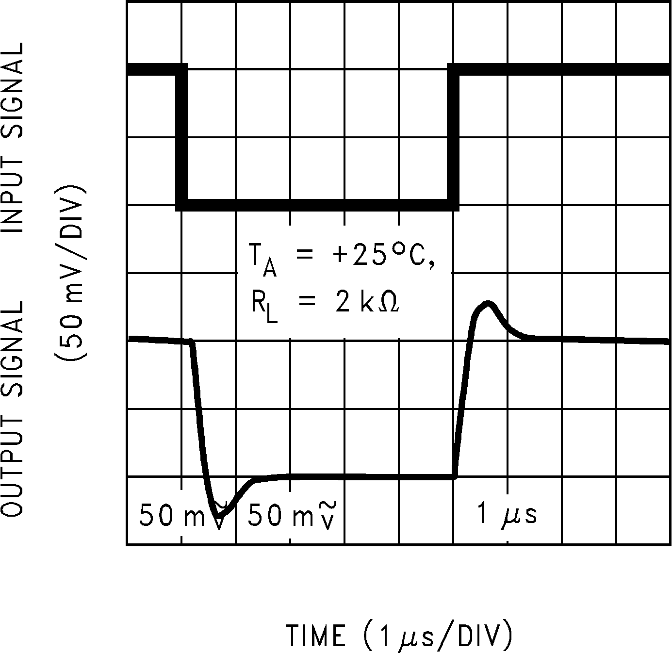 Figure 39. Noninverting Small Signal Pulse Response
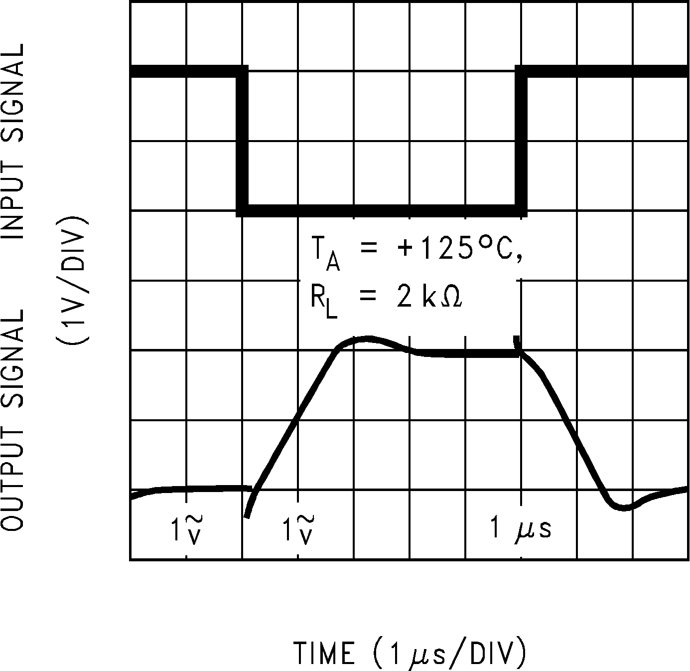 Figure 41. Inverting Large Signal Pulse Response
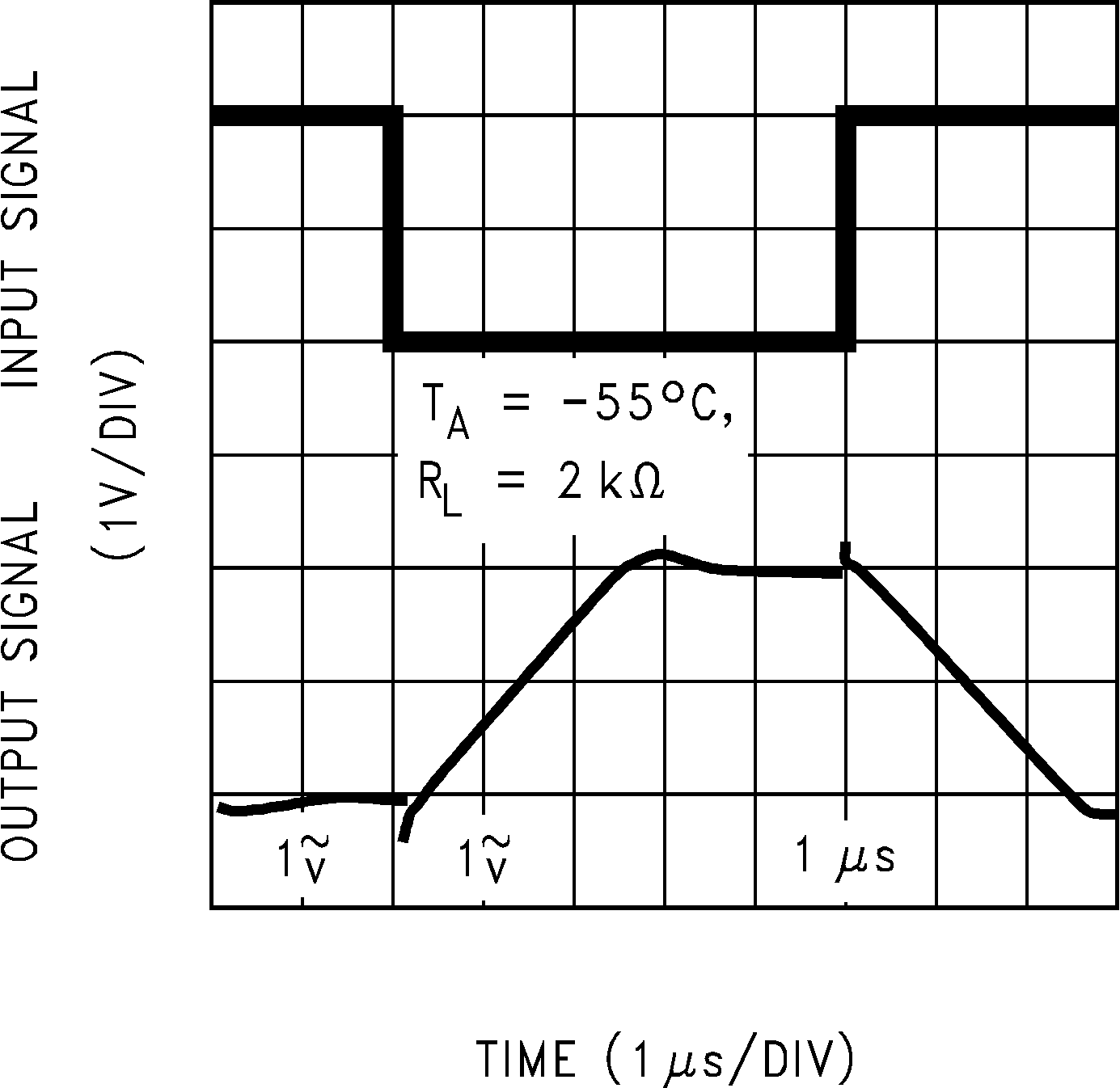 Figure 43. Inverting Large Signal Pulse Response
 Figure 45. Inverting Small Signal Pulse Response
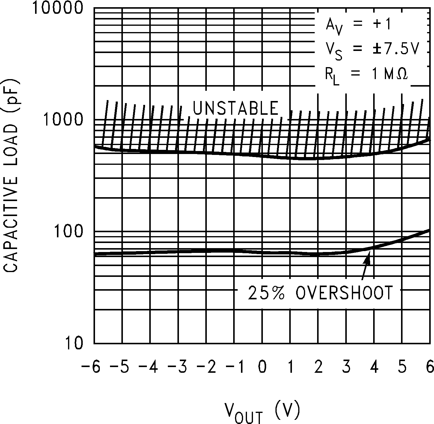 Figure 47. Stability vs. Capacitive Load
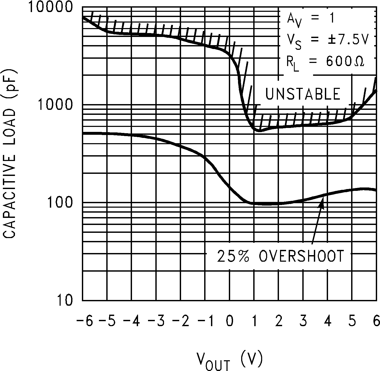 Figure 49. Stability vs. Capacitive Load
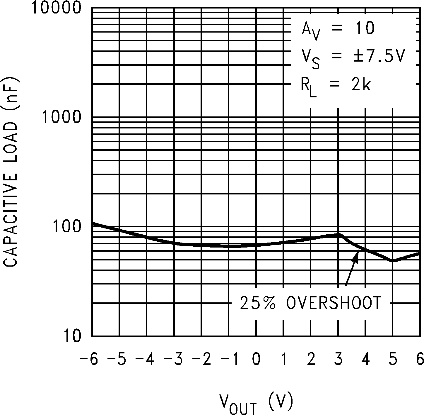 Figure 51. Stability vs. Capacitive Load
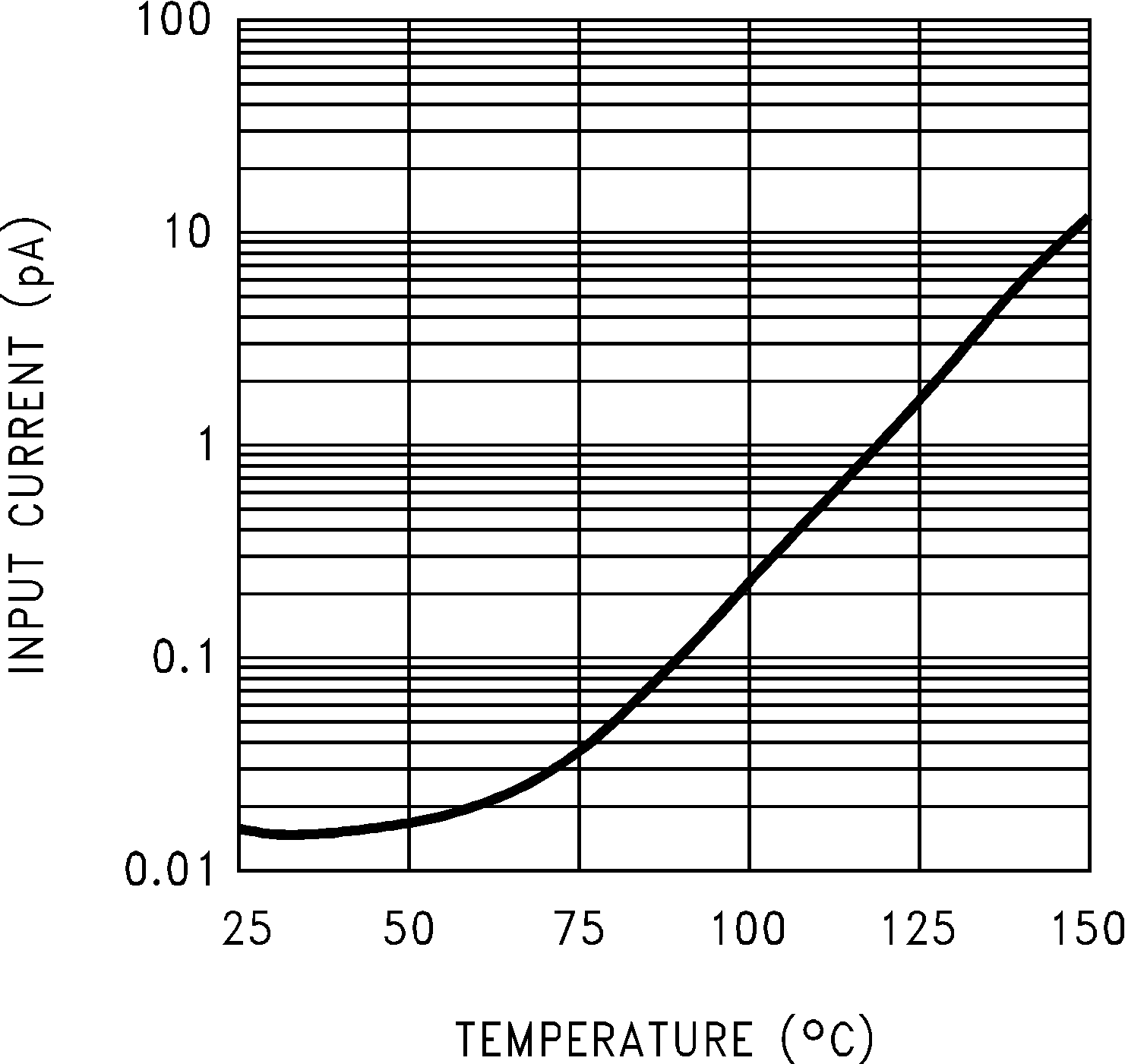 Figure 2. Input Current vs. Temperature
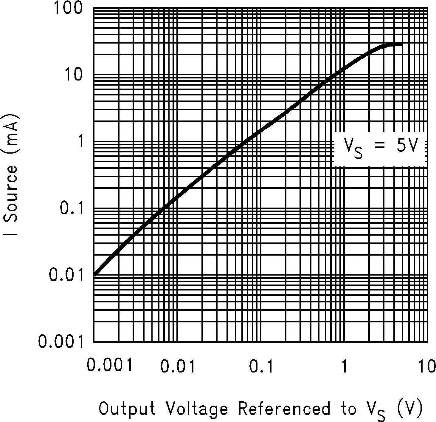 Figure 4. Sourcing Current vs. Output Voltage
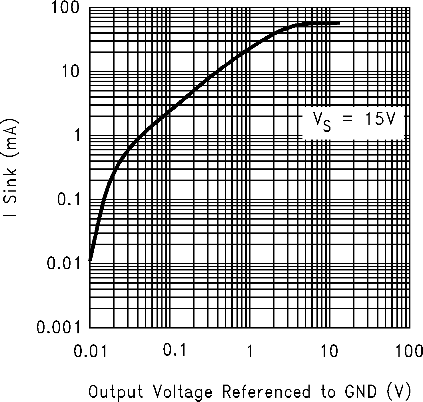 Figure 6. Sinking Current vs. Output Voltage
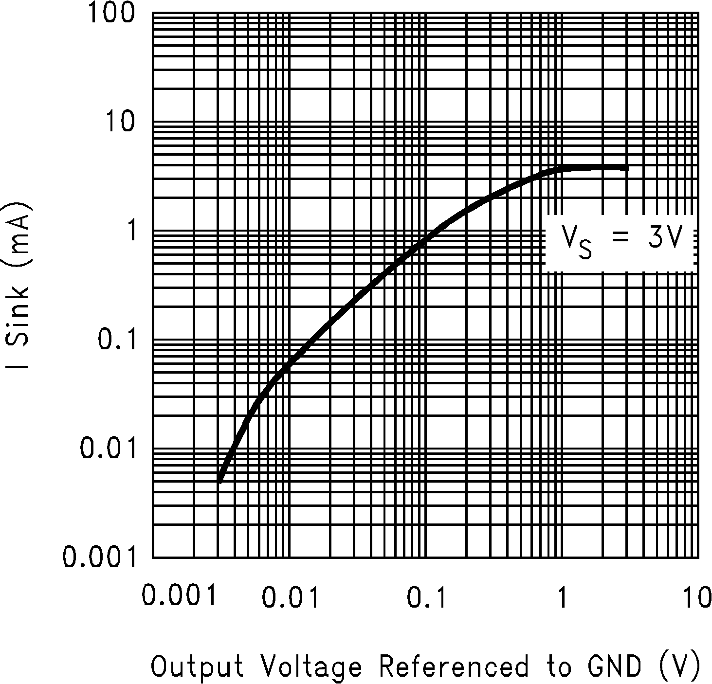 Figure 8. Sinking Current vs. Output Voltage
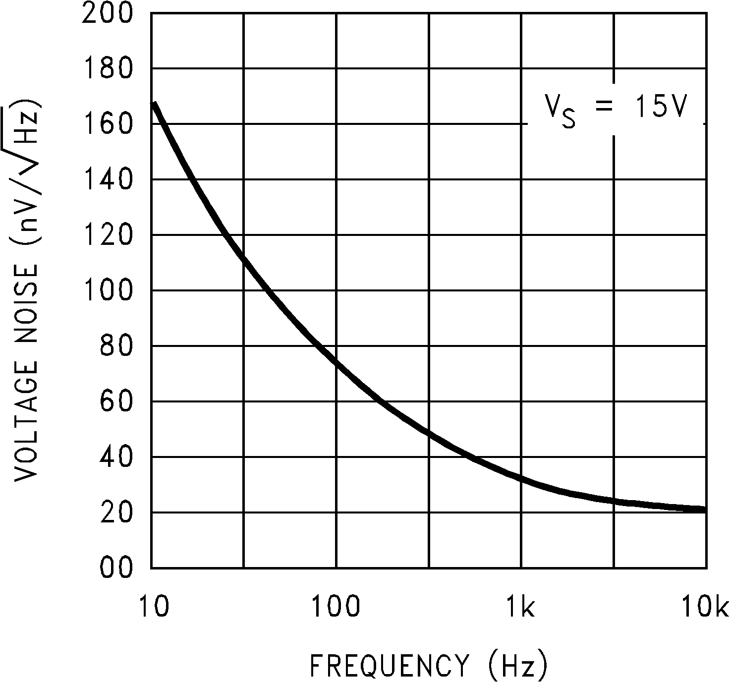 Figure 10. Input Voltage Noise vs. Frequency
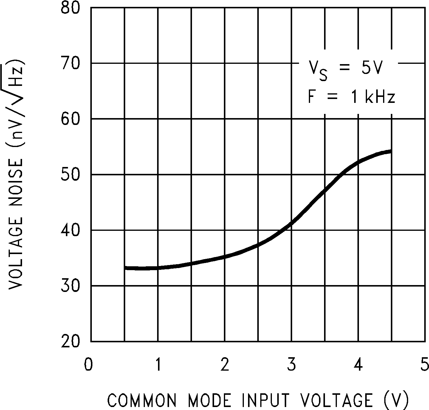 Figure 12. Input Voltage Noise vs. Input Voltage
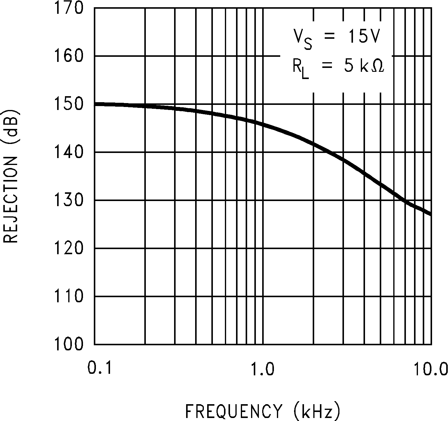 Figure 14. Crosstalk Rejection vs. Frequency
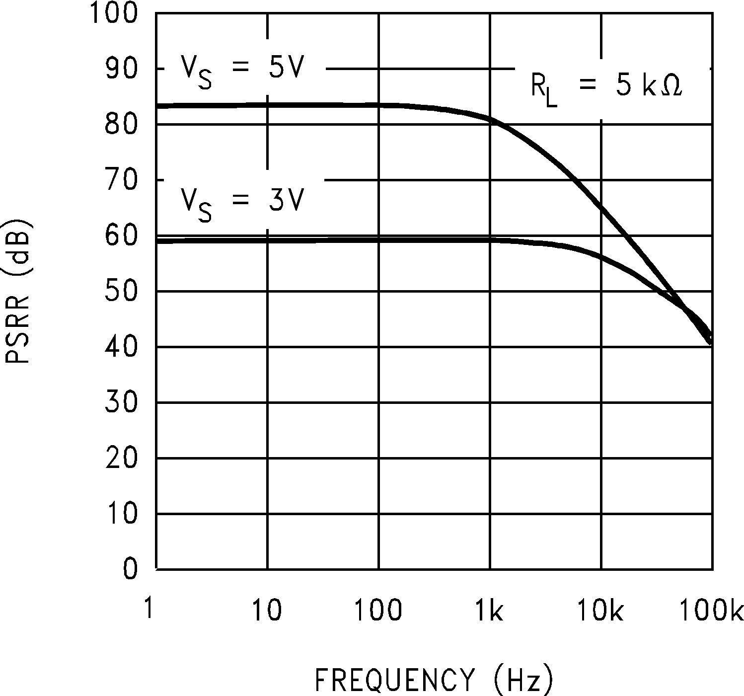 Figure 16. Positive PSRR vs. Frequency
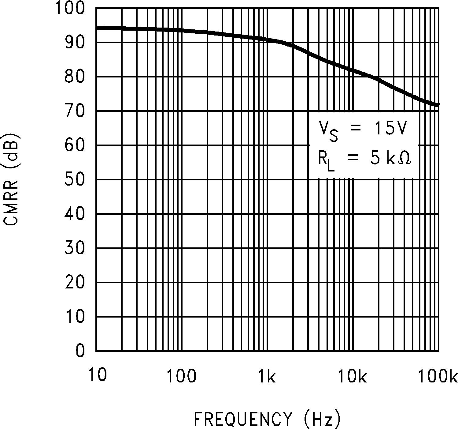 Figure 18. CMRR vs. Frequency
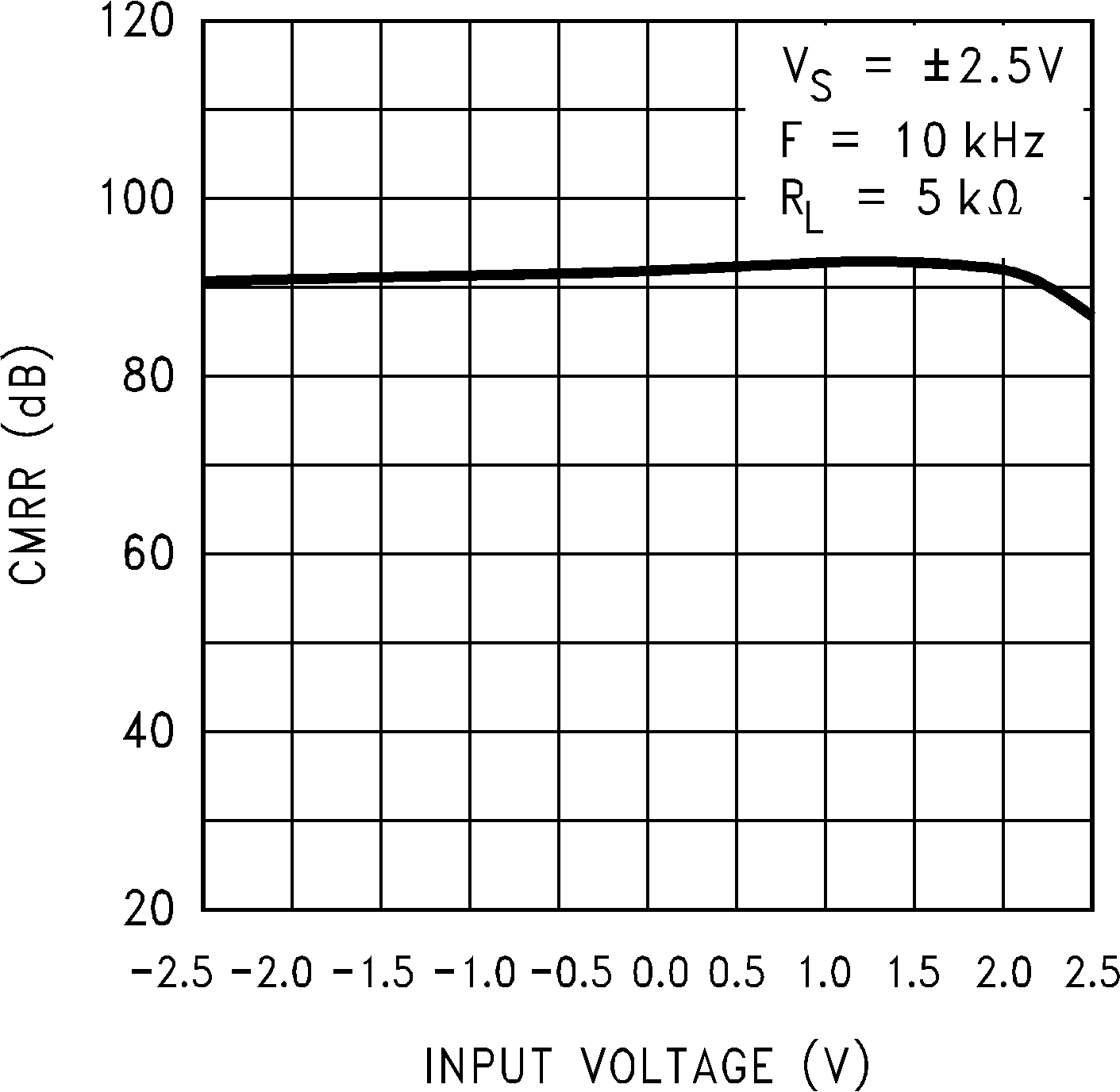 Figure 20. CMRR vs. Input Voltage
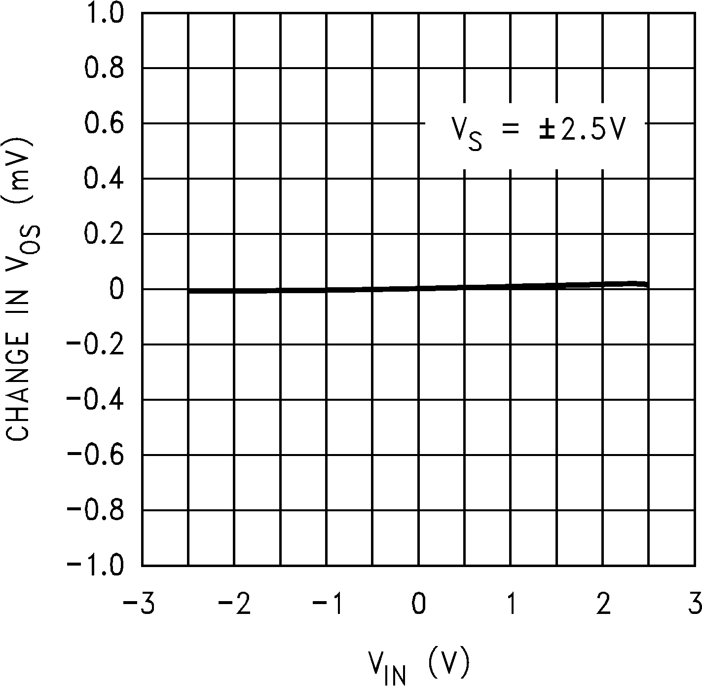 Figure 22. ΔvOS vs. CMR
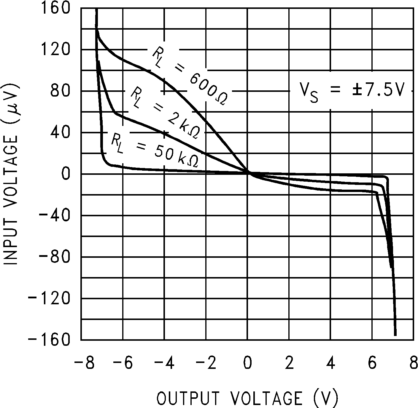 Figure 24. Input Voltage vs. Output Voltage
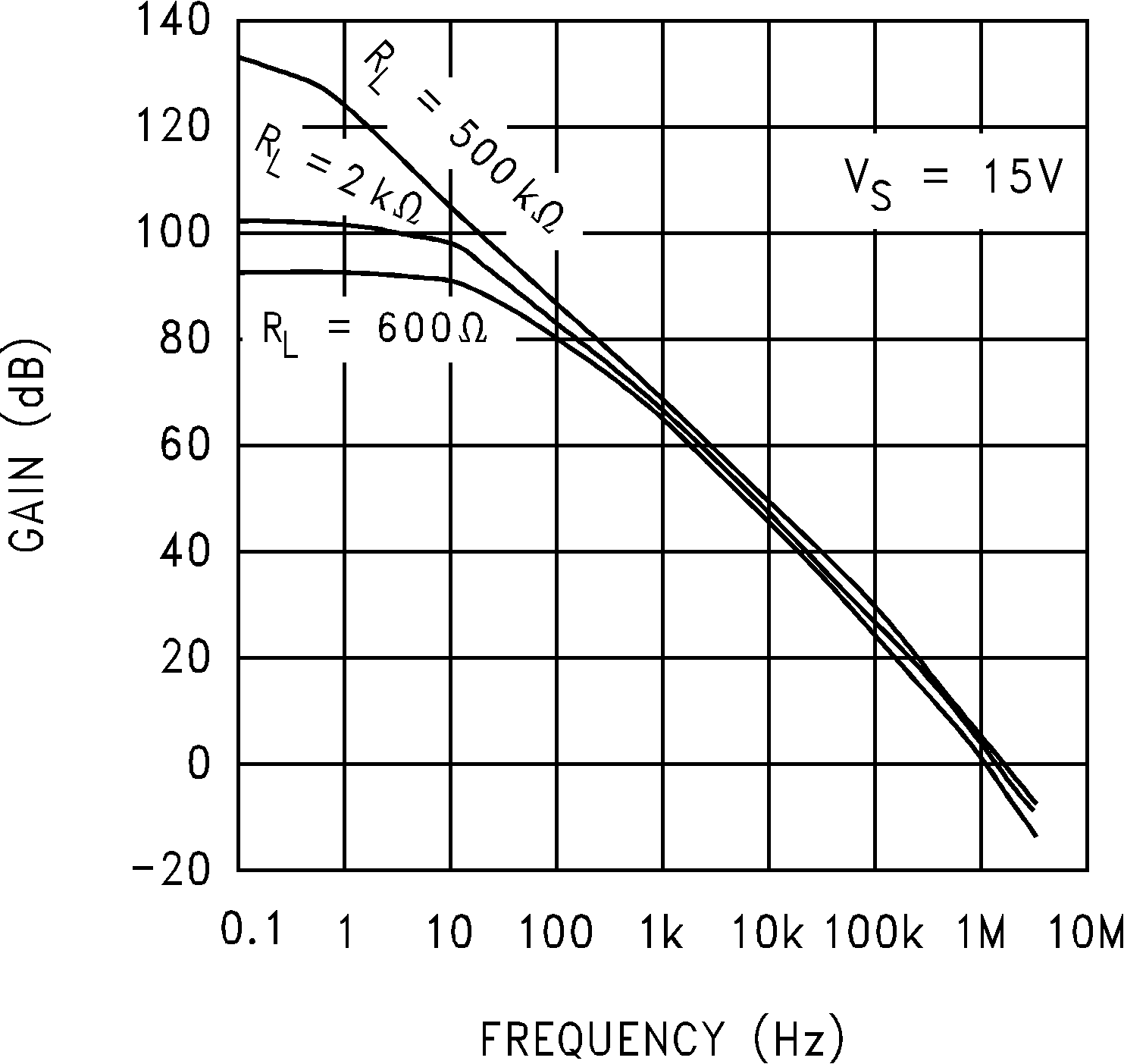 Figure 26. Open-Loop Frequency Response
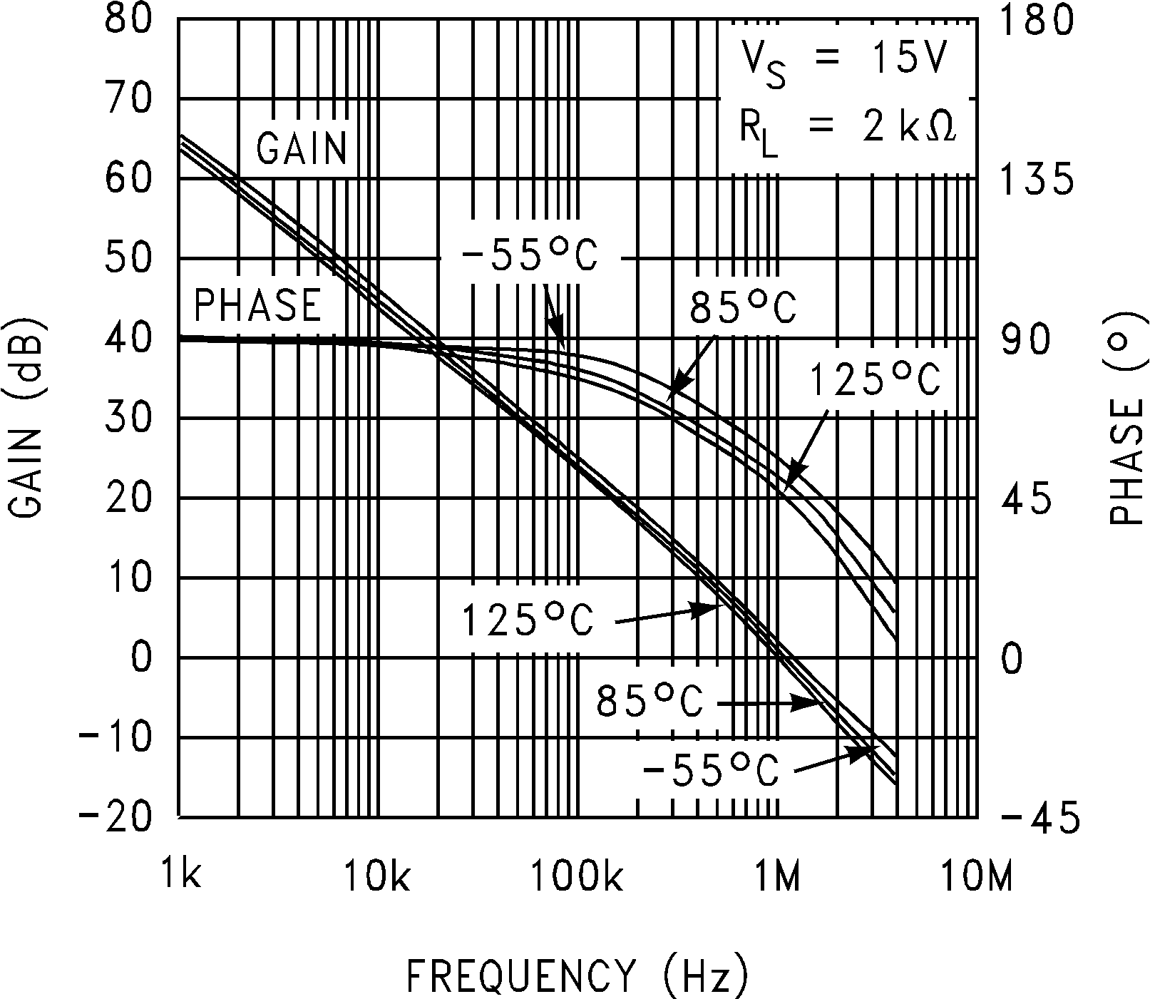 Figure 28. Open-Loop Frequency Response vs. Temperature
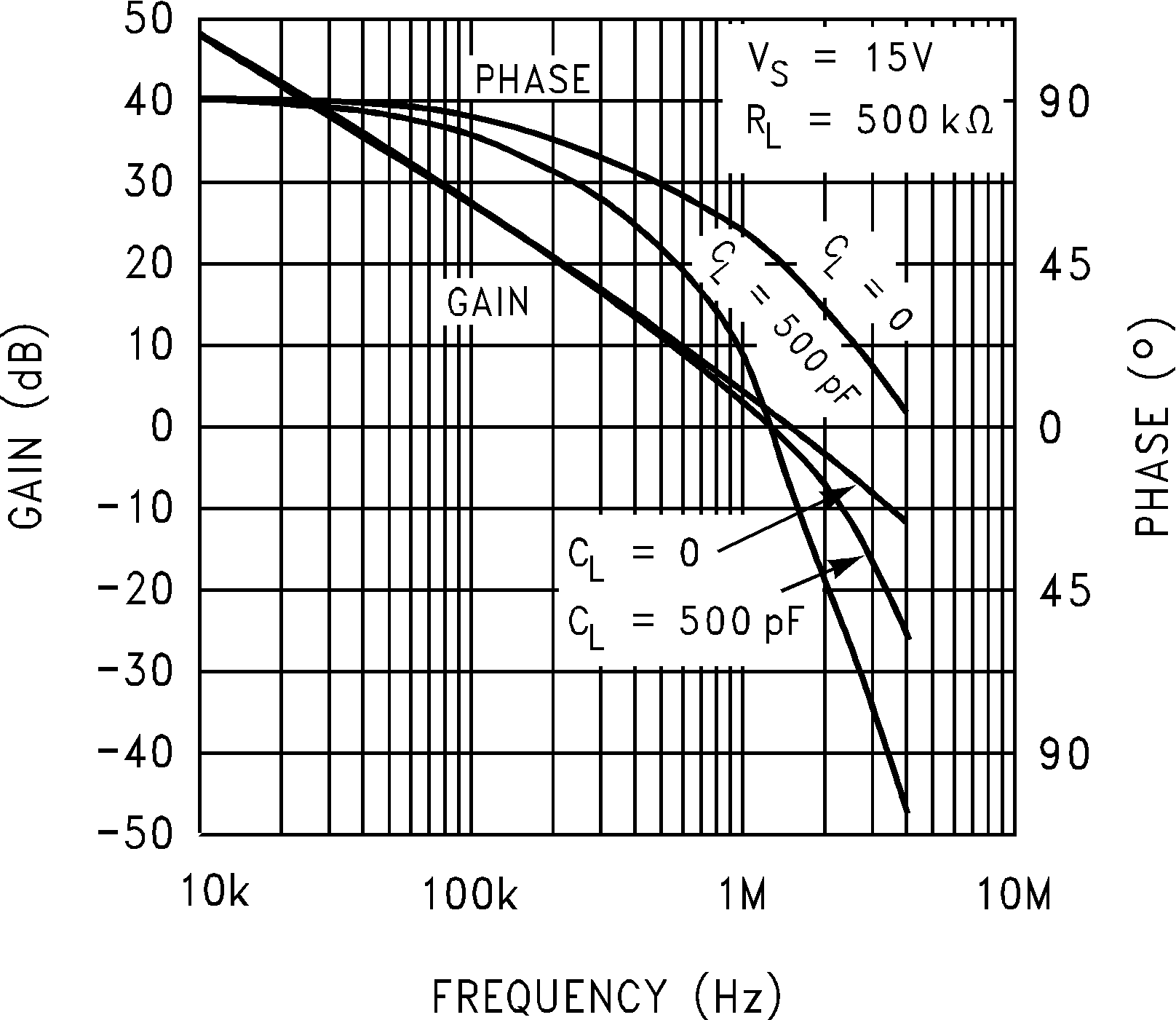 Figure 30. Gain and Phase vs. Capacitive Load
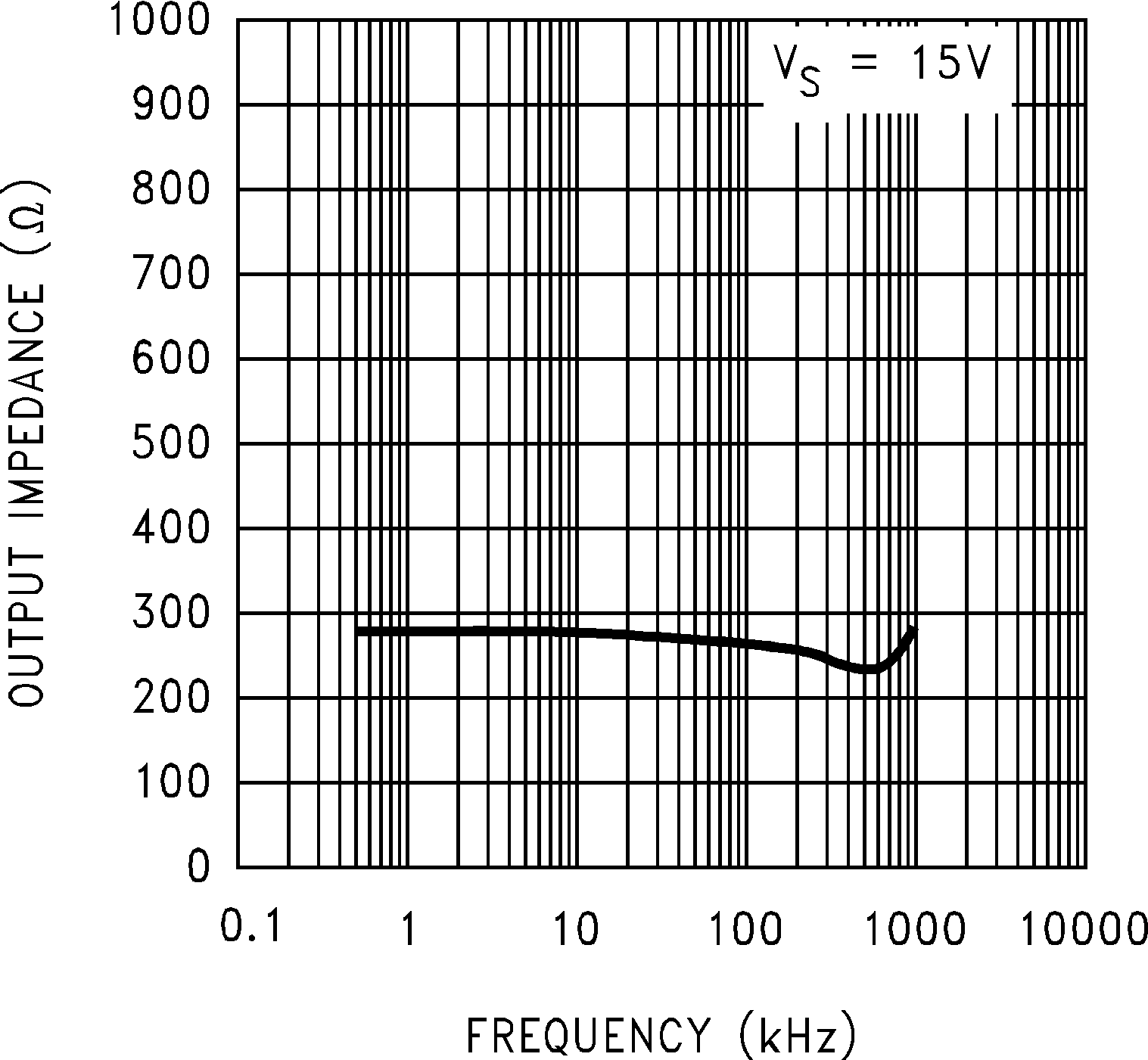 Figure 32. Open-Loop Output Impedance vs. Frequency
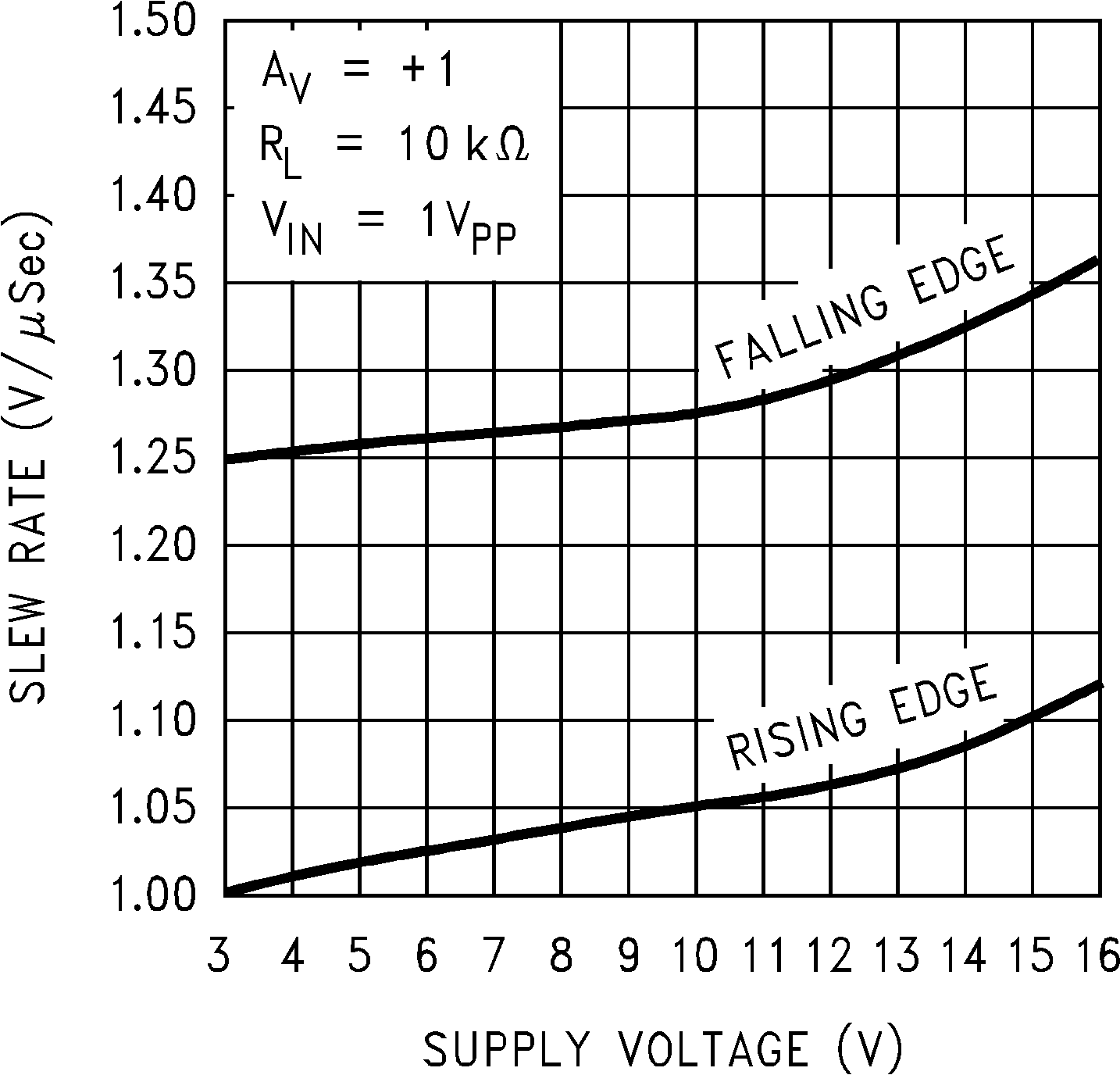 Figure 34. Slew Rate vs. Supply Voltage
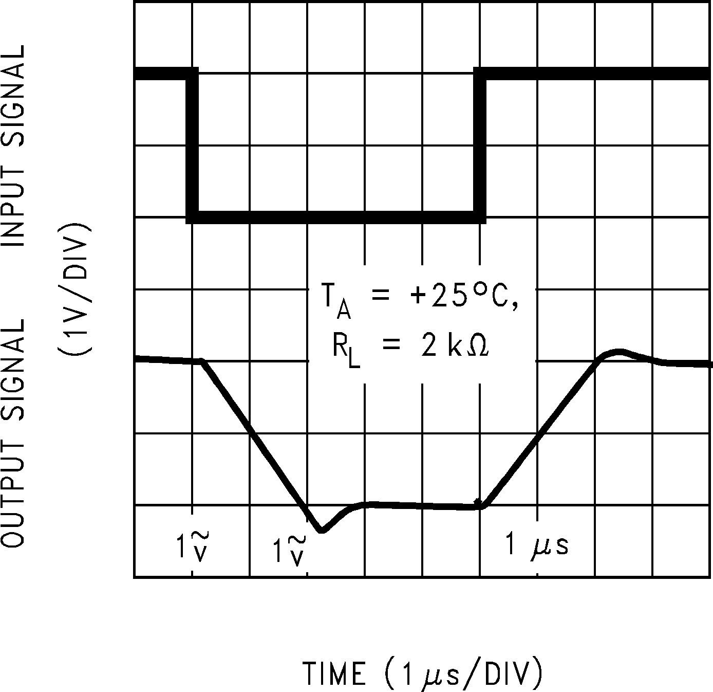 Figure 36. Noninverting Large Signal Pulse Response
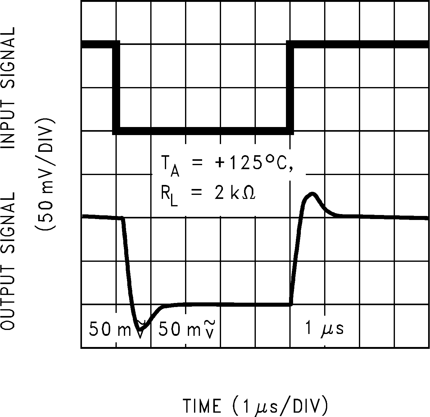 Figure 38. Noninverting Small Signal Pulse Response
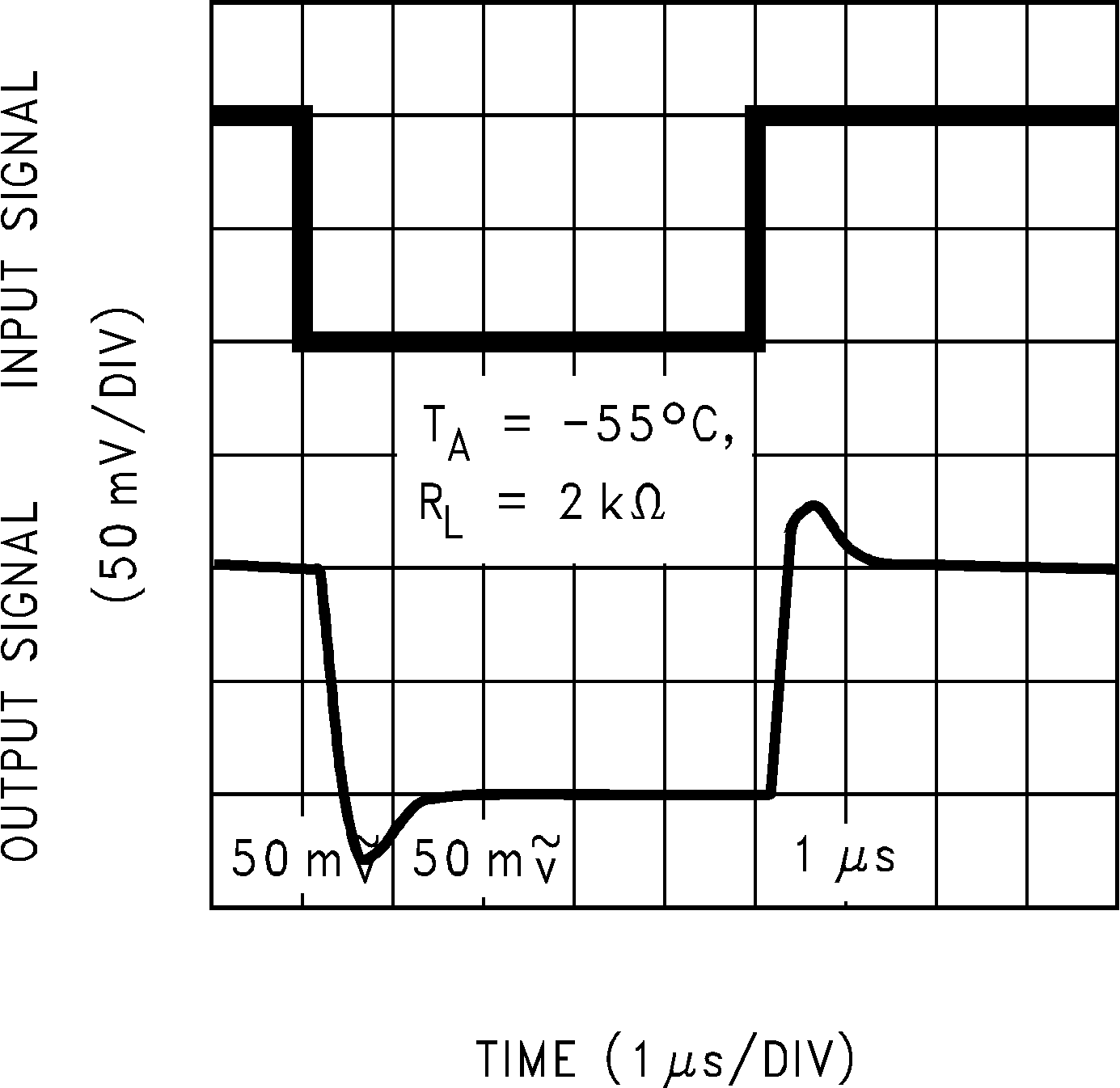 Figure 40. Noninverting Small Signal Pulse Response
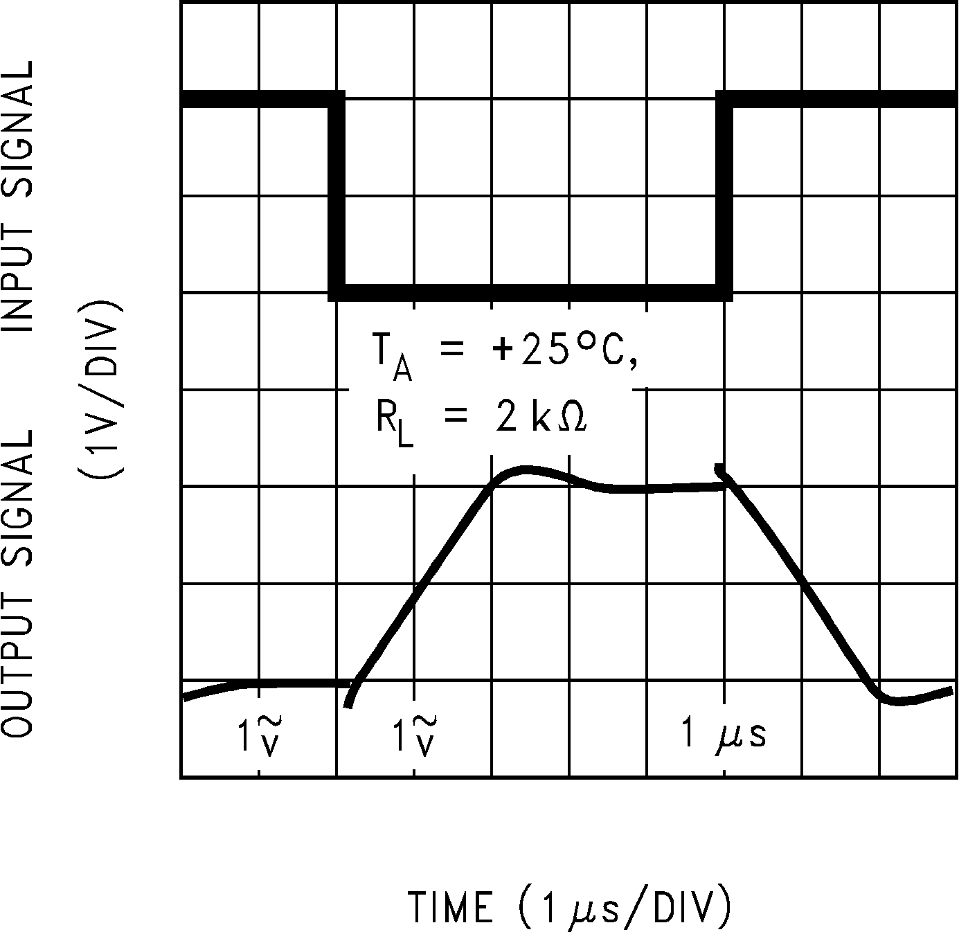 Figure 42. Inverting Large Signal Pulse Response
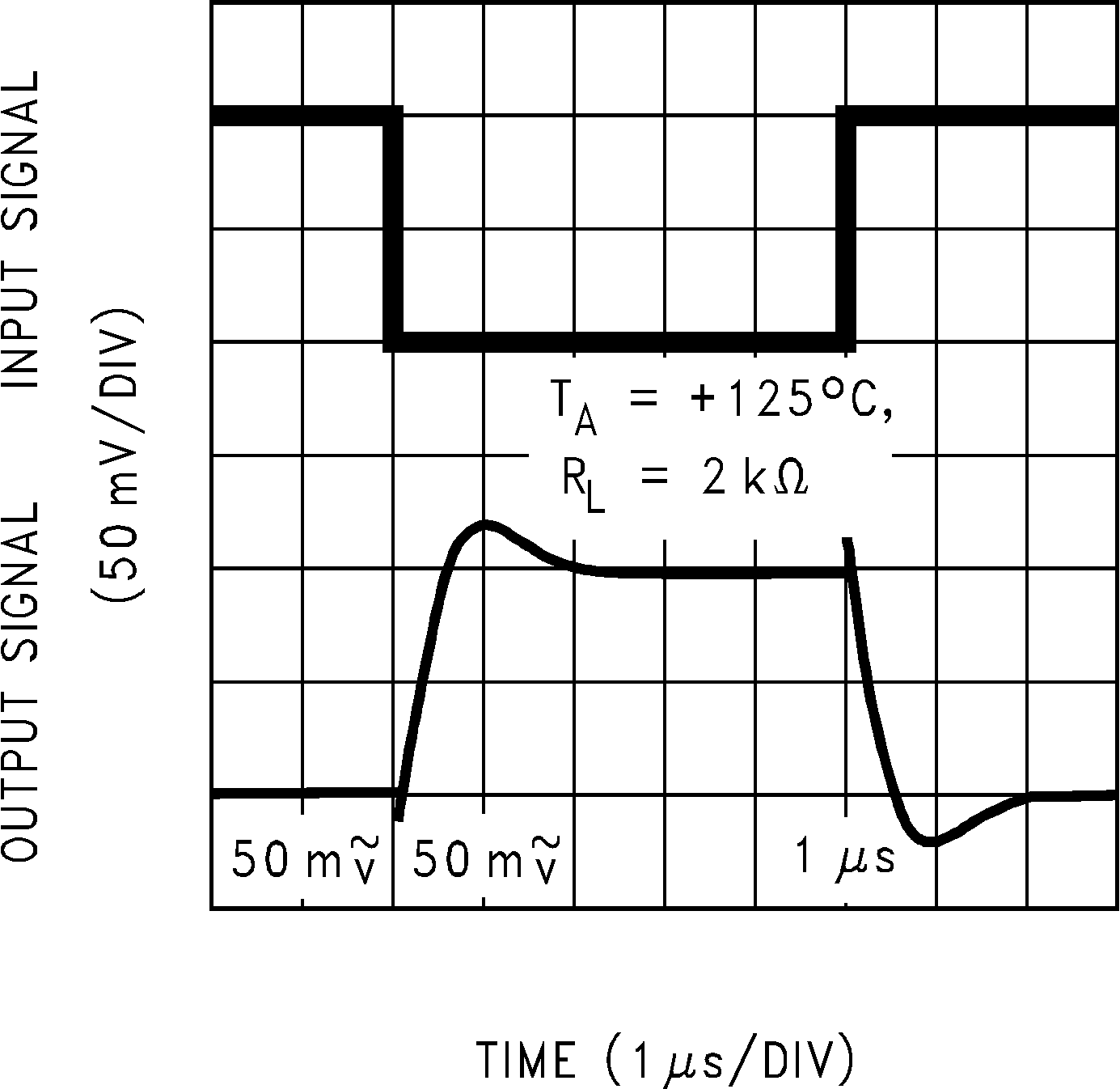 Figure 44. Inverting Small Signal Pulse Response
 Figure 46. Inverting Small Signal Pulse Response
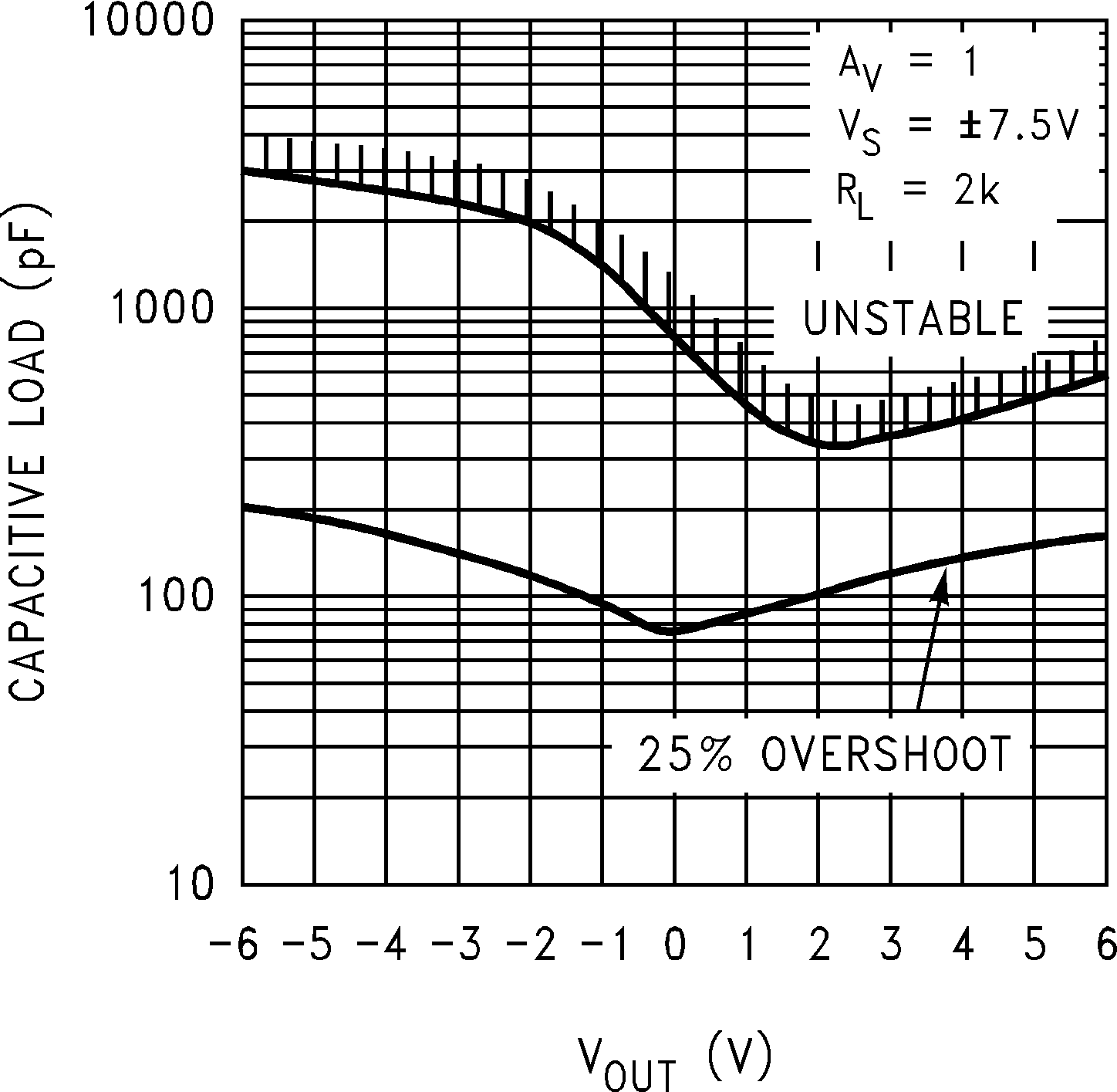 Figure 48. Stability vs. Capacitive Load
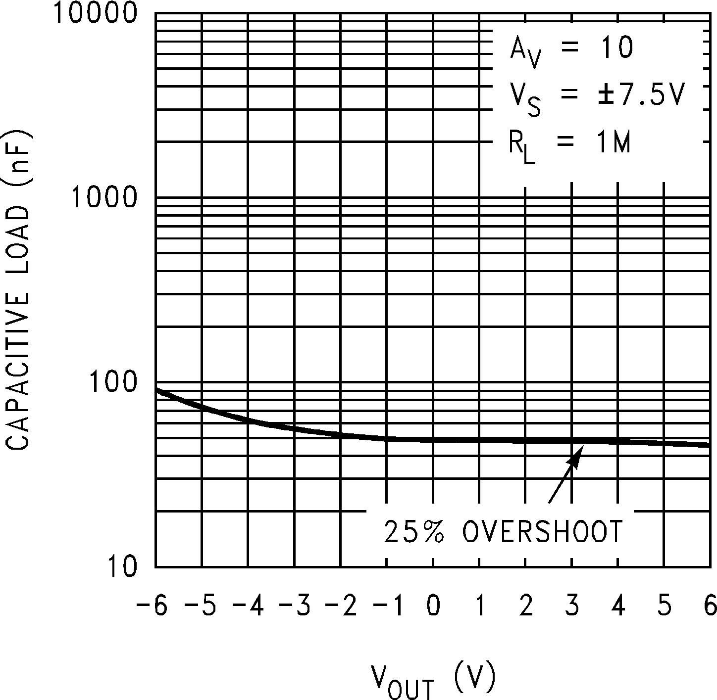 Figure 50. Stability vs. Capacitive Load
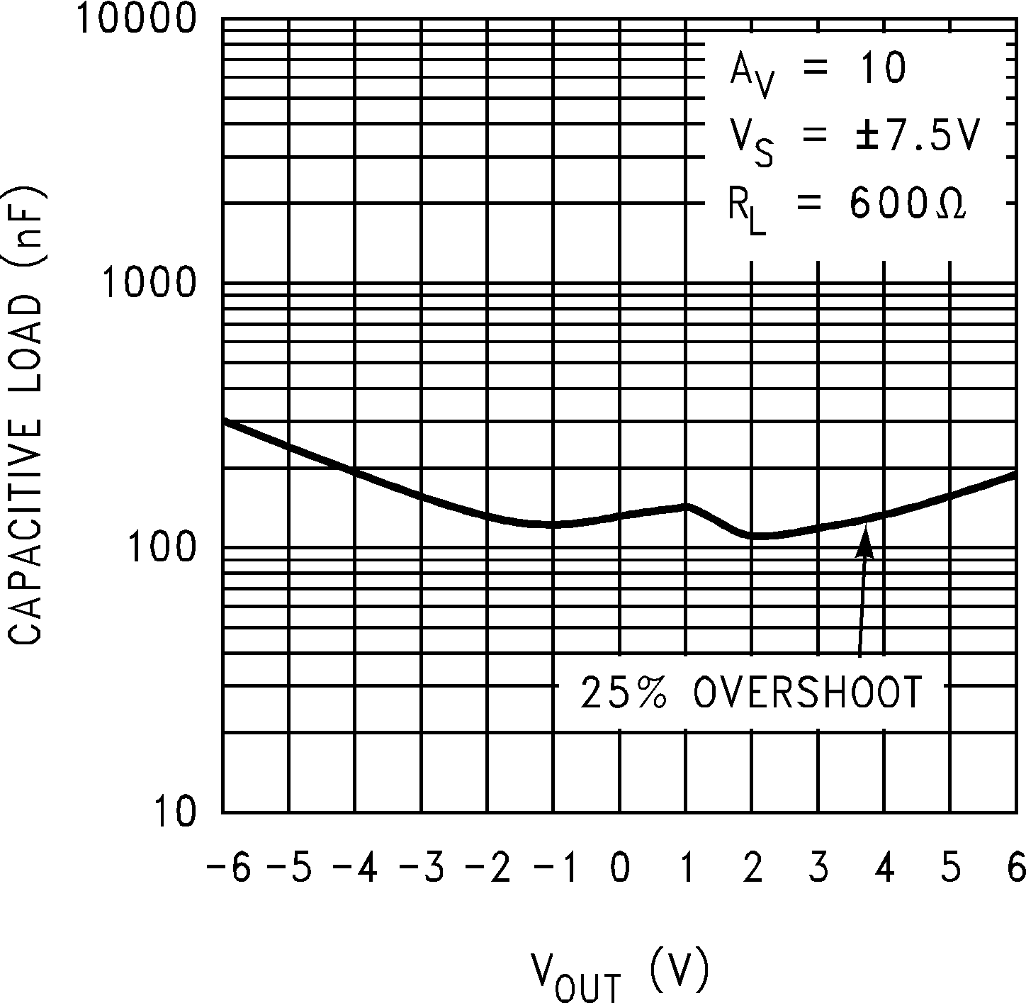 Figure 52. Stability vs. Capacitive Load