JAJSDD7 June 2017 LMC6482-MIL
PRODUCTION DATA.
- 1 特長
- 2 アプリケーション
- 3 概要
- 4 改訂履歴
- 5 Pin Configuration and Functions
- 6 Specifications
- 7 Detailed Description
- 8 Application and Implementation
- 9 Power Supply Recommendations
- 10Layout
- 11デバイスおよびドキュメントのサポート
- 12メカニカル、パッケージ、および注文情報
7 Detailed Description
7.1 Overview
The LMC6482-MIL is a dual CMOS operational amplifier that supports both rail-to-rail inputs and outputs. It may be operated in both dual supply mode and single supply mode.
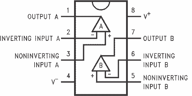
7.2 Functional Block Diagram

7.3 Feature Description
7.3.1 Amplifier Topology
The LMC6482-MIL incorporates specially designed wide-compliance range current mirrors and the body effect to extend input common-mode range to each supply rail. Complementary paralleled differential input stages, like the type used in other CMOS and bipolar rail-to-rail input amplifiers, were not used because of their inherent accuracy problems due to CMRR, crossover distortion, and open-loop gain variation.
The LMC6482-MILs input stage design is complemented by an output stage capable of rail-to-rail output swing even when driving a large load. Rail-to-rail output swing is obtained by taking the output directly from the internal integrator instead of an output buffer stage.
7.3.2 Input Common-Mode Voltage Range
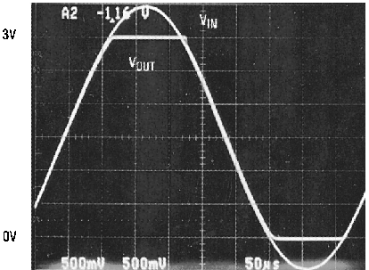
Unlike Bi-FET amplifier designs, the LMC6482-MIL does not exhibit phase inversion when an input voltage exceeds the negative supply voltage. Figure 53 shows an input voltage exceeding both supplies with no resulting phase inversion on the output.

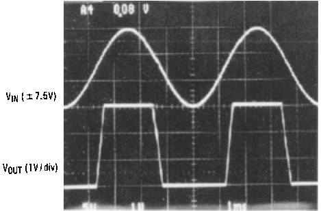
The absolute maximum input voltage is 300 mV beyond either supply rail at room temperature. Voltages greatly exceeding this absolute maximum rating, as in Figure 54, can cause excessive current to flow in or out of the input pins possibly affecting reliability.

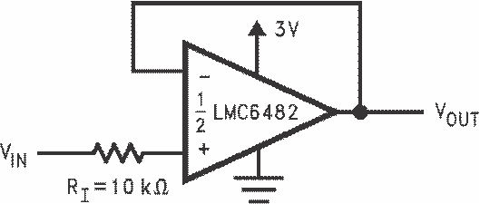
Applications that exceed this rating must externally limit the maximum input current to ±5 mA with an input resistor (RI) as shown in Figure 55.

Voltages Exceeding the Supply Voltages
7.3.3 Rail-to-Rail Output
The approximated output resistance of the LMC6482-MIL is 180-Ω sourcing and 13-0Ω sinking at VS = 3 V and 110-Ω sourcing and 80-Ω sinking at Vs = 5 V. Using the calculated output resistance, maximum output voltage swing can be estimated as a function of load.
7.4 Device Functional Modes
The LMC6482-MIL may be used in applications where each amplifier channel is used independently, or in applications in which the channels are cascaded. See Typical Applications for more information.