JAJSMK7C December   2013  – July 2021 LMK00338

PRODUCTION DATA  

  1. 特長
  2. アプリケーション
  3. 概要
  4. Revision History
  5. Pin Configuration and Functions
  6. Specifications
    1. 6.1 Absolute Maximum Ratings
    2. 6.2 ESD Ratings
    3. 6.3 Recommended Operating Conditions
    4. 6.4 Thermal Information
    5. 6.5 Electrical Characteristics
    6. 6.6 Typical Characteristics
  7. Parameter Measurement Information
    1. 7.1 Differential Voltage Measurement Terminology
  8. Detailed Description
    1. 8.1 Overview
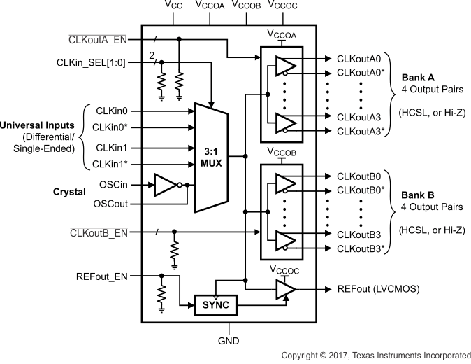
    2. 8.2 Functional Block Diagram
    3. 8.3 Feature Description
      1. 8.3.1 Crystal Power Dissipation vs. RLIM
      2. 8.3.2 Clock Inputs
      3. 8.3.3 Clock Outputs
        1. 8.3.3.1 Reference Output
    4. 8.4 Device Functional Modes
      1. 8.4.1 VCC and VCCO Power Supplies
  9. Power Supply Recommendations
    1. 9.1 Current Consumption and Power Dissipation Calculations
      1. 9.1.1 Power Dissipation Example: Worst-Case Dissipation
    2. 9.2 Power Supply Bypassing
      1. 9.2.1 Power Supply Ripple Rejection
  10. 10Layout
    1. 10.1 Layout Guidelines
    2. 10.2 Layout Example
    3. 10.3 Thermal Management
  11. 11Device and Documentation Support
    1. 11.1 Documentation Support
      1. 11.1.1 Related Documentation
    2. 11.2 ドキュメントの更新通知を受け取る方法
    3. 11.3 サポート・リソース
    4. 11.4 Trademarks
    5. 11.5 静電気放電に関する注意事項
    6. 11.6 用語集

パッケージ・オプション

メカニカル・データ(パッケージ|ピン)
サーマルパッド・メカニカル・データ
発注情報

Functional Block Diagram

GUID-DF6AB0DF-038F-4875-BB30-44D392B4D7AA-low.gif