SNAS642A June 2014 – July 2014 LMK00804B
PRODUCTION DATA.
- 1 Features
- 2 Applications
- 3 Description
- 4 Simplified Schematic
- 5 Device Comparison Table
- 6 Pin Configuration and Functions
-
7 Specifications
- 7.1 Pin Characteristics
- 7.2 Absolute Maximum Ratings
- 7.3 Handling Ratings
- 7.4 Recommended Operating Conditions
- 7.5 Thermal Information
- 7.6 Power Supply Characteristics
- 7.7 LVCMOS / LVTTL DC Characteristics
- 7.8 Differential Input DC Characteristics
- 7.9 Electrical Characteristics (VDDO = 3.3 V ± 5%)
- 7.10 Electrical Characteristics (VDDO = 2.5 V ± 5%)
- 7.11 Electrical Characteristics (VDDO = 1.8 V ± 0.15 V)
- 7.12 Electrical Characteristics (VDDO = 1.5 V ± 5%)
- 7.13 Typical Characteristics
- 8 Parameter Measurement Information
- 9 Detailed Description
- 10Applications and Implementation
- 11Power Supply Recommendations
- 12Layout
- 13Device and Documentation Support
- 14Mechanical, Packaging, and Orderable Information
9 Detailed Description
9.1 Overview
The LMK00804B is a low skew, high performance clock fanout buffer which can distribute up to four LVCMOS/LVTTL outputs (3.3-V, 2.5-V, 1.8-V, or 1.5-V levels) from one of two selectable inputs, which can accept differential or single-ended inputs. The clock enable input is synchronized internally to eliminate runt or glitch pulses on the outputs when the clock enable terminal is asserted or de-asserted. The outputs are held in logic low state when the clock is disabled. A separate output enable terminal controls whether the outputs are active state or high-impedance state. The low additive jitter and phase noise floor, and guaranteed output and part-to-part skew characteristics make the LMK00804B ideal for applications demanding high performance and repeatability.
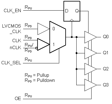
9.2 Functional Block Diagram
9.2.1
9.3 Feature Description
9.3.1 Clock Enable Timing
After CLK_EN switches, the clock outputs are disabled or enabled following a rising and falling input clock edge as shown in Figure 8. In the enabled mode, the output states are a function of the CLK/nCLK or LVCMOS_CLK inputs as described in Clock Input Function.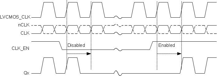 Figure 8. Clock Enable Timing Diagram
9.4 Device Functional Modes
The device can provide fan-out and level translation from differential or single-ended input to LVCMOS/LVTTL output, where the output VOH and VOL levels are determined by the VDDO output supply voltage and output load condition. Refer to the Clock Input Function.
9.4.1 Clock Input Function
Table 1.
| INPUTS | OUTPUTS | INPUT to OUTPUT MODE | POLARITY | |
|---|---|---|---|---|
| CLK (or LVCMOS_CLK) | nCLK | Qx | ||
| 0 | 1 | LOW | Differential (or Single-Ended) to Single-Ended | Non-inverting |
| 1 | 0 | HIGH | Differential (or Single-Ended) to Single-Ended | Non-inverting |
| 0 | Floating or Biased | LOW | Single-Ended to Single-Ended | Non-inverting |
| 1 | Floating or Biased | HIGH | Single-Ended to Single-Ended | Non-inverting |
| Biased | 0 | HIGH | Single-Ended to Single-Ended | Inverting |
| Biased | 1 | LOW | Single-Ended to Single-Ended | Inverting |