SNAS642A June 2014 – July 2014 LMK00804B
PRODUCTION DATA.
- 1 Features
- 2 Applications
- 3 Description
- 4 Simplified Schematic
- 5 Device Comparison Table
- 6 Pin Configuration and Functions
-
7 Specifications
- 7.1 Pin Characteristics
- 7.2 Absolute Maximum Ratings
- 7.3 Handling Ratings
- 7.4 Recommended Operating Conditions
- 7.5 Thermal Information
- 7.6 Power Supply Characteristics
- 7.7 LVCMOS / LVTTL DC Characteristics
- 7.8 Differential Input DC Characteristics
- 7.9 Electrical Characteristics (VDDO = 3.3 V ± 5%)
- 7.10 Electrical Characteristics (VDDO = 2.5 V ± 5%)
- 7.11 Electrical Characteristics (VDDO = 1.8 V ± 0.15 V)
- 7.12 Electrical Characteristics (VDDO = 1.5 V ± 5%)
- 7.13 Typical Characteristics
- 8 Parameter Measurement Information
- 9 Detailed Description
- 10Applications and Implementation
- 11Power Supply Recommendations
- 12Layout
- 13Device and Documentation Support
- 14Mechanical, Packaging, and Orderable Information
12 Layout
12.1 Layout Guidelines
12.1.1 Ground Planes
Solid ground planes are recommended as they provide a low-impedance return paths between the device and its bypass capacitors and its clock source and destination devices.
Avoid return paths of other system circuitry (for example, high-speed/digital logic, switching power supplies, and so forth) from passing through the local ground of the device to minimize noise coupling, which could induce added jitter and spurious noise.
12.1.2 Power Supply Pins
Follow the power supply schematic and layout example described in Power-Supply Filtering.
12.1.3 Differential Input Termination
- Place input termination or biasing resistors as close as possible to the CLK/nCLK pins.
- Avoid or minimize vias in the 50 Ω input traces to minimize impedance discontinuities. Intra-pair skew should be also be minimized on the differential input traces.
- If not used, CLK/nCLK inputs may be left floating.
12.1.4 LVCMOS Input Termination
- When the LVCMOS_CLK input is driven from a LVCMOS driver that is series terminated to match the characteristic impedance of the trace, then input termination is not necessary; otherwise, place the input termination resistor as close as possible to the LVCMOS_CLK input.
- Avoid or minimize vias in the 50 Ω input trace to minimize impedance discontinuities.
- If not used, LVCMOS_CLK input may be left floating.
12.1.5 Output Termination
- Place 43 Ω series termination resistors as close as possible to the Qx outputs at the launch of the 50 Ω traces.
- Avoid or minimize vias in the 50 Ω input traces to minimize impedance discontinuities.
- If not used, any Qx output should be left floating and not routed.
12.2 Layout Example
Please refer to the LMK00804BEVM for a layout example. A sample PCB layer is shown below.
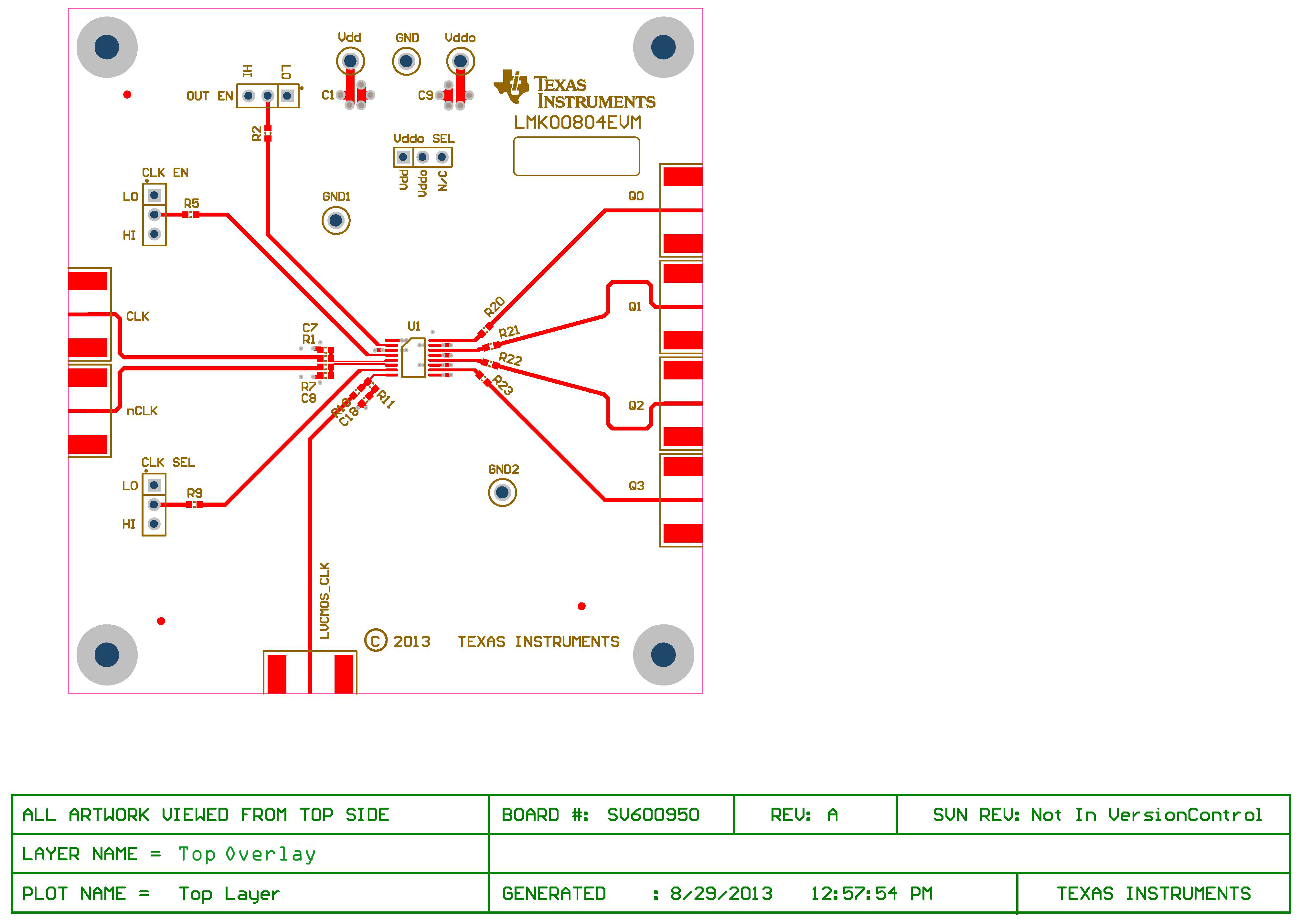 Figure 21. Sample PCB Layout, Layer 1 (Top View)