JAJSJN5B december 2020 – june 2023 LMK1D1204 , LMK1D1208
PRODUCTION DATA
- 1
- 1 特長
- 2 アプリケーション
- 3 概要
- 4 Revision History
- 5 Device Comparison
- 6 Pin Configuration and Functions
- 7 Specifications
- 8 Parameter Measurement Information
- 9 Detailed Description
- 10Application and Implementation
- 11Device and Documentation Support
- 12Mechanical, Packaging, and Orderable Information
パッケージ・オプション
メカニカル・データ(パッケージ|ピン)
- RGT|16
サーマルパッド・メカニカル・データ
- RGT|16
発注情報
9.4.2 Input Termination
The LMK1D120x input stage is designed with flexibility in mind to allow the user to drive the device with a wide variety of signal types. This device can be interfaced with LVDS, LVPECL, LP-HCSL, HCSL, CML or LVCMOS drivers. Please refer to Electrical Characteristics for more details.
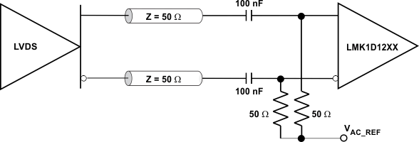
LVDS drivers can be connected to LMK1D120x inputs with DC- and AC-coupling as shown Figure 9-3 and Figure 9-4 (respectively).
 Figure 9-3 LVDS
Clock Driver Connected to LMK1D120x Input (DC-Coupled)
 Figure 9-4 LVDS
Clock Driver Connected to LMK1D120x Input (AC-Coupled)
Figure 9-4 LVDS
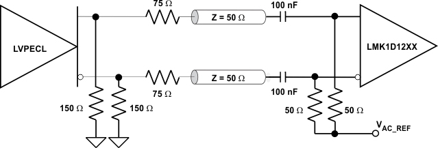
Clock Driver Connected to LMK1D120x Input (AC-Coupled)Figure 9-5 shows how to connect LVPECL inputs to the LMK1D120x. The series resistors are required to reduce the LVPECL signal swing if the signal swing is >1.6 VPP.
 Figure 9-5 LVPECL
Clock Driver Connected to LMK1D120x Input
Figure 9-5 LVPECL
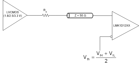
Clock Driver Connected to LMK1D120x InputFigure 9-6 illustrates how to couple a LVCMOS clock input to the LMK1D120x directly.
 Figure 9-6 1.8-V/2.5-V/3.3-V LVCMOS Clock Driver Connected to LMK1D120x Input
For unused input, TI recommends grounding both input pins (INP, INN) using 1-kΩ resistors.