JAJSO15A february 2022 – june 2023 LMK1D1208I
PRODUCTION DATA
- 1
- 1 特長
- 2 アプリケーション
- 3 概要
- 4 Revision History
- 5 Device Comparison
- 6 Pin Configuration and Functions
- 7 Specifications
- 8 Parameter Measurement Information
- 9 Detailed Description
- 10Application and Implementation
- 11Device and Documentation Support
- 12Mechanical, Packaging, and Orderable Information
パッケージ・オプション
メカニカル・データ(パッケージ|ピン)
- RHA|40
サーマルパッド・メカニカル・データ
- RHA|40
発注情報
8 Parameter Measurement Information
 Figure 8-1 LVDS Output DC Configuration During Device Test
 Figure 8-2 LVDS Output AC Configuration During Device Test
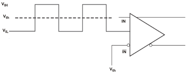
 Figure 8-3 DC-Coupled LVCMOS Input During Device Test
 Figure 8-4 Output Voltage and Rise/Fall Time
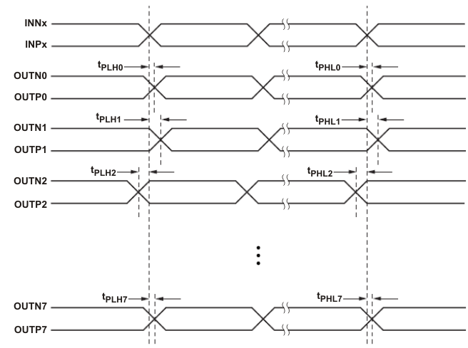
A. Output skew is calculated as the greater of the following: the difference between the fastest and the slowest tPLHn or the difference between the fastest and the slowest tPHLn (n = 0, 1, 2, ..7)
B. Part-to-part skew is calculated as the greater of the following: the difference between the fastest and the slowest tPLHn or the difference between the fastest and the slowest tPHLn across multiple devices (n = 0, 1, 2, ..7)
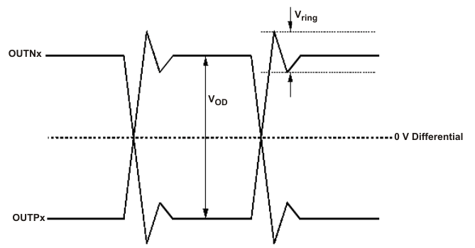
Figure 8-5 Output Skew and Part-to-Part Skew Figure 8-6 Output Overshoot and Undershoot
 Figure 8-7 Output AC Common Mode