JAJSIO5B July 2019 – February 2020 LMR36506-Q1
ADVANCE INFORMATION for pre-production products; subject to change without notice.
- 1 特長
- 2 アプリケーション
- 3 概要
- 4 改訂履歴
- 5 Device Comparison Table
- 6 Pin Configuration and Functions
- 7 Specifications
-
8 Detailed Description
- 8.1 Overview
- 8.2 Functional Block Diagram
- 8.3
Feature Description
- 8.3.1 Output Voltage Selection
- 8.3.2 Enable and Start-up
- 8.3.3 External CLK SYNC (with MODE/SYNC)
- 8.3.4 Adjustable Switching Frequency (with RT)
- 8.3.5 Power-Good Flag Output
- 8.3.6 Internal LDO, VCC UVLO, and VOUT/BIAS Input
- 8.3.7 Bootstrap Voltage and VCBOOT-UVLO (CBOOT Terminal)
- 8.3.8 Spread Spectrum
- 8.3.9 Soft Start and Recovery from Dropout
- 8.3.10 Current Limit and Short Circuit
- 8.3.11 Thermal Shutdown
- 8.4 Device Functional Modes
-
9 Application and Implementation
- 9.1 Application Information
- 9.2
Typical Application
- 9.2.1 Design Requirements
- 9.2.2 Detailed Design Procedure
- 9.3 What to Do and What Not to Do
- 10Power Supply Recommendations
- 11Layout
- 12デバイスおよびドキュメントのサポート
- 13メカニカル、パッケージ、および注文情報
パッケージ・オプション
メカニカル・データ(パッケージ|ピン)
- RPE|9
サーマルパッド・メカニカル・データ
- RPE|9
発注情報
8.3.2 Enable and Start-up
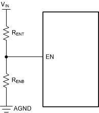
Voltage on the EN pin controls the ON or OFF functionality of the LMR36506-Q1. The part stays in shutdown mode as long as the EN pin voltage is less than VEN-WAKE = 0.4 V. During the shutdown mode, the input current drawn by the device typically drops down to 1 µA. Applying a voltage at the EN pin greater than the VEN-WAKE causes the device to enter the standby mode, powering up the internal LDO to generate VCC. As the EN voltage further approaches VEN-VOUT, the device finally starts switching, allowing it to enter the start-up mode and begin the soft-start period. During the shutdown process, when the EN input is brought below VEN-VOUT by VEN-HYST, the regulator stops switching and re-enters the standby mode. Any further decrease in the EN pin voltage below VEN-WAKE finally shuts down the device. The EN input pin can be connected directly to VIN input pin if remote precision control is not needed. The EN input pin must not be allowed to float. The limits of various EN thresholds values listed here can be found in the Electrical Characteristics table.
 Figure 2. VIN UVLO Using the EN pin