JAJSIO5B July 2019 – February 2020 LMR36506-Q1
ADVANCE INFORMATION for pre-production products; subject to change without notice.
- 1 特長
- 2 アプリケーション
- 3 概要
- 4 改訂履歴
- 5 Device Comparison Table
- 6 Pin Configuration and Functions
- 7 Specifications
-
8 Detailed Description
- 8.1 Overview
- 8.2 Functional Block Diagram
- 8.3
Feature Description
- 8.3.1 Output Voltage Selection
- 8.3.2 Enable and Start-up
- 8.3.3 External CLK SYNC (with MODE/SYNC)
- 8.3.4 Adjustable Switching Frequency (with RT)
- 8.3.5 Power-Good Flag Output
- 8.3.6 Internal LDO, VCC UVLO, and VOUT/BIAS Input
- 8.3.7 Bootstrap Voltage and VCBOOT-UVLO (CBOOT Terminal)
- 8.3.8 Spread Spectrum
- 8.3.9 Soft Start and Recovery from Dropout
- 8.3.10 Current Limit and Short Circuit
- 8.3.11 Thermal Shutdown
- 8.4 Device Functional Modes
-
9 Application and Implementation
- 9.1 Application Information
- 9.2
Typical Application
- 9.2.1 Design Requirements
- 9.2.2 Detailed Design Procedure
- 9.3 What to Do and What Not to Do
- 10Power Supply Recommendations
- 11Layout
- 12デバイスおよびドキュメントのサポート
- 13メカニカル、パッケージ、および注文情報
パッケージ・オプション
メカニカル・データ(パッケージ|ピン)
- RPE|9
サーマルパッド・メカニカル・データ
- RPE|9
発注情報
8.3.9.1 Recovery from Dropout
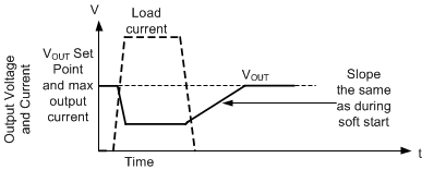
Any time output voltage is more than a few percent low for any reason, output voltage slowly ramps up. This condition, called graceful recovery from dropout in this document, differs from soft start in two important ways:
- FPWM mode is allowed during recovery from dropout. If output voltage were to suddenly be pulled up by an external supply, the LMR36506-Q1 can pull down on the output. Note that all protections that are present during normal operation are in place, preventing destruction if output is shorted to a high voltage or ground.
- The reference voltage is set to approximately 1% above that needed to achieve the current output voltage. It is not started from zero.
 Figure 6. Recovery from Dropout
 Whether output voltage falls due to high load or low input voltage, once the condition that causes output to fall below its set point is removed, output climbs at the same speed as during start-up.