SNOS534J February 2001 – November 2016 LMV712-N , LMV712-N-Q1
PRODUCTION DATA.
- 1 Features
- 2 Applications
- 3 Description
- 4 Revision History
- 5 Pin Configuration and Functions
- 6 Specifications
- 7 Detailed Description
- 8 Application and Implementation
- 9 Power Supply Recommendations
- 10Layout
- 11Device and Documentation Support
- 12Mechanical, Packaging, and Orderable Information
8 Application and Implementation
NOTE
Information in the following applications sections is not part of the TI component specification, and TI does not warrant its accuracy or completeness. TI’s customers are responsible for determining suitability of components for their purposes. Customers should validate and test their design implementation to confirm system functionality.
8.1 Application Information
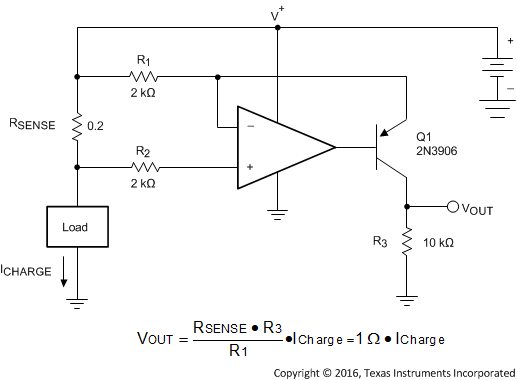
The LMV712-N devices are dual op amps derived from the LMV711 single op amp. Figure 34 contains a simplified schematic of one channel of the LMV712-N.
8.2 Typical Applications
8.2.1 High-Side Current-Sensing
 Figure 34. High-Side, Current-Sensing Schematic
8.2.1.1 Design Requirements
The high-side, current-sensing circuit (Figure 34) is commonly used in a battery charger to monitor charging current to prevent over charging. A sense resistor RSENSE is connected to the battery directly. This system requires an op amp with rail-to-rail input. The LMV712-N is ideal for this application because its common-mode input range goes up to the rail.
8.2.1.2 Detailed Design Procedure
As seen in (Figure 34), the ICHARGE current flowing through sense resistor RSENSE develops a voltage drop equal to VSENSE. The voltage at the negative sense point is now less than the positive sense point by an amount proportional to the VSENSE voltage.
The low-bias currents of the LMV712-N causes little voltage drop through R2, so the negative input of the LMV712-N amplifier is at essentially the same potential as the negative sense input.
The LMV712-N detects this voltage error between its inputs and servo the transistor base to conduct more current through Q1, increasing the voltage drop across R1 until the LMV712-N inverting input matches the noninverting input. At this point, the voltage drop across R1 now matches VSENSE.
IG, a current proportional to ICHARGE, flows according to Equation 1.
IG also flows through the gain resistor R3 developing a voltage drop equal to Equation 2.
where
- G = R3 / R1
The other channel of the LMV712-N may be used to buffer the voltage across R3 to drive the following stages.
8.2.1.3 Application Curve
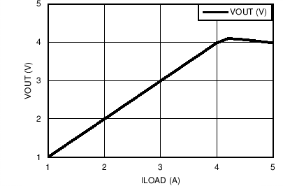
 Figure 35. High-Side Current-Sensing Results
8.2.2 Peak Detector
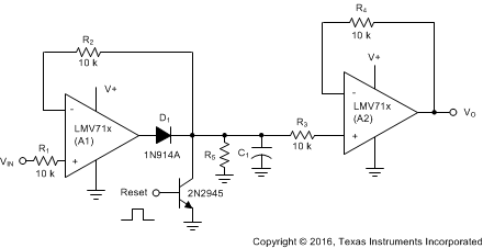
 Figure 36. Peak Detector Schematic
8.2.2.1 Design Requirements
A peak detector outputs a DC voltage equal to the peak value of the applied AC signal. Peak detectors are used in many applications, such as test equipment, measurement instrumentation, ultrasonic alarm systems, and so forth. Figure 36 shows the schematic diagram of a peak detector using LMV712-N. This peak detector basically consists of a clipper, a parallel RC network, and a voltage follower.
8.2.2.2 Detailed Design Procedure
An AC voltage source applied to VIN charges capacitor C1 to the peak of the input. Diode D1 conducts positive half cycles, charging C1 to the waveform peak. Including D1 inside the feedback loop of the amplifier removes the voltage drop of D1 and allows an accurate peak detection of VIN on C1. When the input waveform falls below the DC peak stored on C1, D1 is reverse biased. The low input bias current of A1 and the reverse biasing of D1 limits current leakage from C1. As a result, C1 retains the peak value even as the waveform drops to zero. A2 further isolates the peak value on C1 while completing the peak detector circuit by operating as a voltage follower and reporting the peak voltage of C1 at its output.
R5 and C1 are properly selected so that the capacitor is charged rapidly to VIN. During the holding period, the capacitor slowly discharge through C1, through leakage of the capacitor and the reverse-biased diode, or op amp bias currents. In any cases the discharging time constant is much larger than the charge time constant. And the capacitor can hold its voltage long enough to minimize the output ripple.
Resistors R2 and R3 limit the current into the inverting input of A1 and the noninverting input of A2 when power is disconnected from the circuit. The discharging current from C1 during power off may damage the input circuitry of the op amps.
The peak detector is reset by applying a positive pulse to the reset transistor. The charge on the capacitor is dumped into ground, and the detector is ready for another cycle.
The maximum input voltage to this detector must be less than (V+ – VD), where VD is the forward voltage drop of the diode. Otherwise, the input voltage must be scaled down before applying to the circuit.
8.2.3 GSM Power Amplifier Control Loop
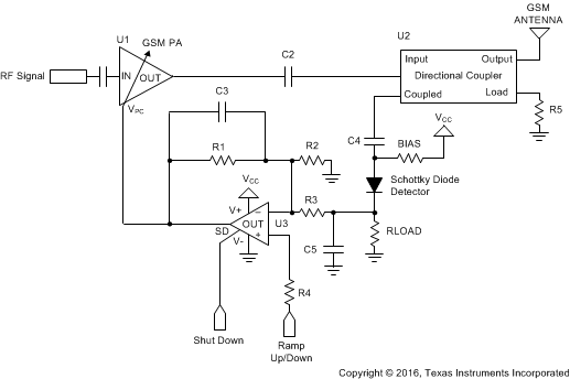
 Figure 37. GSM Power Amplifier Control Loop Schematic
8.2.3.1 Design Requirements
The control loop in Figure 37 controls the output power level of a GSM mobile phones. The control loop is used to avoid intermodulation of base station receivers, to prevent intermodulation with other mobile phones, and to minimize power consumption depending on the distance between mobile and base station.
8.2.3.2 Detailed Design Procedure
There are four critical sections in the GSM Power Amplifier Control Loop. The class-C RF power amplifier provides amplification of the RF signal. A directional coupler couples small amount of RF energy from the output of the RF P. A. to an envelope detector diode. The detector diode senses the signal level and rectifies it to a DC level to indicate the signal strength at the antenna. An op amp is used as an error amplifier to process the diode voltage and ramping voltage. This loop control the power amplifier gain through the op amp and forces the detector diode voltage and ramping voltage to be equal. Power control is accomplished by changing the ramping voltage.
The LMV712-N is well suited as an error amplifier in this application. The LMV712-N has an extra shutdown pin to switch the op amp to shutdown mode. In shutdown mode, the LMV712-N consumes very low current. Therefore, the power amplifier can be turned off to save battery life. The LMV712-N output is tri-stated when in shutdown.