SNOS534J February 2001 – November 2016 LMV712-N , LMV712-N-Q1
PRODUCTION DATA.
- 1 Features
- 2 Applications
- 3 Description
- 4 Revision History
- 5 Pin Configuration and Functions
- 6 Specifications
- 7 Detailed Description
- 8 Application and Implementation
- 9 Power Supply Recommendations
- 10Layout
- 11Device and Documentation Support
- 12Mechanical, Packaging, and Orderable Information
7 Detailed Description
7.1 Overview
The LMV712-N features low voltage, low power, and rail-to-rail output operational amplifiers designed for low-voltage portable applications.
7.2 Functional Block Diagram

7.3 Feature Description
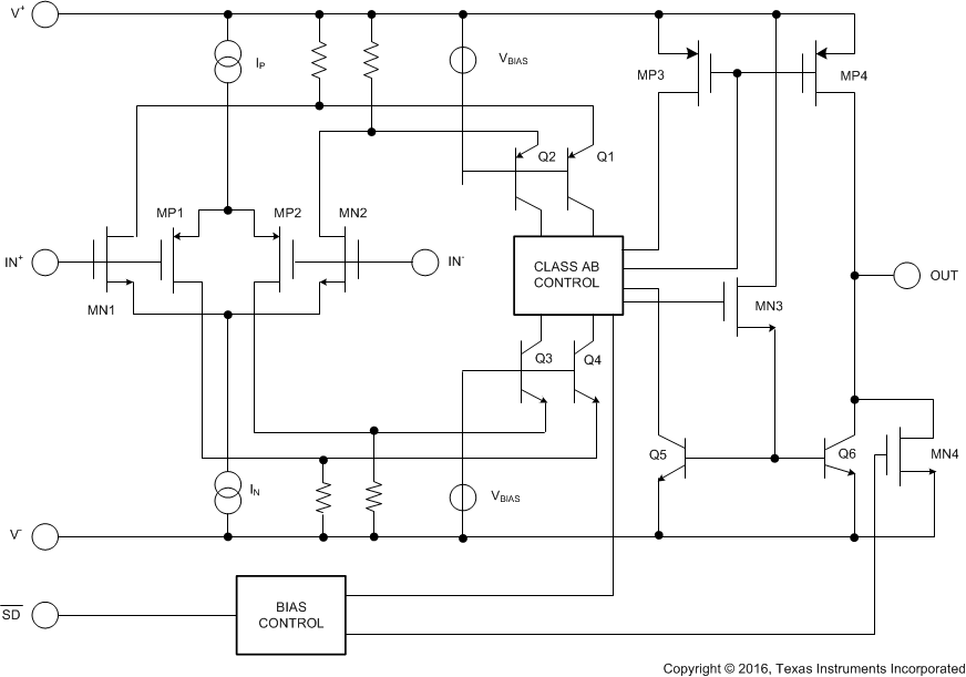
Rail-to-rail input is achieved by using in parallel, one NMOS differential pair (MN1 and MN2) and one PMOS differential pair (MP1 and MP2). When the common mode input voltage (VCM) is near V+, the NMOS pair is on and the PMOS pair is off. When VCM is near V−, the NMOS pair is off and the PMOS pair is on. When VCM is between V+ and V−, internal logic decides how much current each differential pair receives. This special logic ensures stable and low distortion amplifier operation within the entire common mode voltage range.
Because both input stages have their own offset voltage (VOS) characteristic, the offset voltage of the LMV712-N becomes a function of VCM. VOS has a crossover point at 1.4 V above V− (see Figure 3). Caution must be taken in situations where input signal amplitude is comparable to VOS value or the design requires high accuracy. In these situations, it is necessary for the input signal to avoid the crossover point.
The current coming out of the input differential pairs gets mirrored through two folded cascode stages (Q1, Q2, Q3, Q4) into the class AB control block. This circuitry generates voltage gain, defines the dominant pole of the op amp and limits the maximum current flowing at the output stage. MN3 introduces a voltage level shift and acts as a high impedance to low impedance buffer.
The output stage is composed of a PMOS and a NPN transistor in a common source or emitter configuration, delivering a rail-to-rail output excursion.
The MN4 transistor ensures that the LMV712-N output remains near V− when the amplifier is in shutdown mode.
7.4 Device Functional Modes
7.4.1 Shutdown Pin
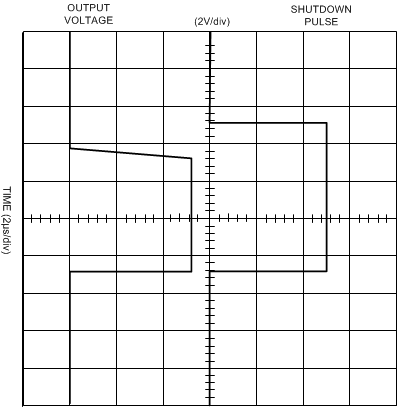
The LMV712-N offers independent shutdown pins for the dual amplifiers. When the shutdown pin is tied low, the respective amplifier shuts down and the supply current is reduced to less than 1 µA. In shutdown mode, the output level of the amplifier stays at V−. In a 2.7-V operation, when a voltage from 1.5 V to 2.7 V is applied to the shutdown pin, the amplifier is enabled. As the amplifier is coming out of the shutdown mode, the output waveform ramps up without any glitch.
 Figure 31. Output Recovery from Shutdown
A glitch-free output waveform is highly desirable in many applications, one of which is power amplifier control loops. In this application, the LMV712-N is used to drive the power amplifier's power control. If the LMV712-N did not have a smooth output ramp during turn on, it would directly cause the power amplifier to produce a glitch at its output. This adversely affects the performance of the system.
To enable the amplifier, the shutdown pin must be pulled high. It must not be left floating in the event that any leakage current may inadvertently turn off the amplifier.
7.4.2 Capacitive Load Tolerance
The LMV712-N can directly drive 200 pF in unity-gain without oscillation. The unity-gain follower is the most sensitive configuration to capacitive loading. Direct capacitive loading reduces the phase margin of amplifiers. The combination of the amplifier's output impedance and the capacitive load induces phase lag. This results in either an underdamped pulse response or oscillation. To drive a heavier capacitive load, TI recommends the circuit in Figure 32.
 Figure 32. Driving Heavy Capacitive Loads
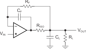
In Figure 32, the isolation resistor RISO and the load capacitor CL form a pole to increase stability by adding more phase margin to the overall system. The desired performance depends on the value of RISO. The bigger the RISO resistor value, the more stable VOUT is. But the DC accuracy is degraded when the RISO gets bigger. If there were a load resistor in the application, the output voltage would be divided by RISO and the load resistor.
Figure 33 is an improvement to the one in Figure 32 because it provides DC accuracy as well as AC stability. In Figure 33, RF provides the DC accuracy by using feed-forward techniques to connect VIN to RL. CF and RISO serve to counteract the loss of phase margin by feeding the high frequency component of the output signal back to the inverting input of the amplifier, thereby preserving phase margin in the overall feedback loop. Increased capacitive drive is possible by increasing the value of CF. This in turn slows down the pulse response.
 Figure 33. Enhanced DC Accuracy
7.4.3 Latchup
CMOS devices tend to be susceptible to latchup due to their internal parasitic SCR (silicon controlled rectifier) effects. The input and output pins look similar to the gate of the SCR. There is a minimum current required to trigger the SCR gate lead. The LMV712-N is designed to withstand 150-mA surge current on all the pins. Some resistive method must be used to isolate any capacitance from supplying excess current to the pins. In addition, like an SCR, there is a minimum holding current for any latchup mode. Limiting current to the supply pins also inhibits latchup susceptibility.