SNOSAI3D October 2006 – September 2015 LMV951
PRODUCTION DATA.
8 Application and Implementation
NOTE
Information in the following applications sections is not part of the TI component specification, and TI does not warrant its accuracy or completeness. TI’s customers are responsible for determining suitability of components for their purposes. Customers should validate and test their design implementation to confirm system functionality.
8.1 Application Information
The unique internal charge pumps allows the LMV951 to fully function at supply voltages as low as 0.9 V. This opens up new possibilities for unique low-voltage circuits that are not possible with standard amplifiers.
8.2 Typical Applications
8.2.1 Two Wire Line Transmission
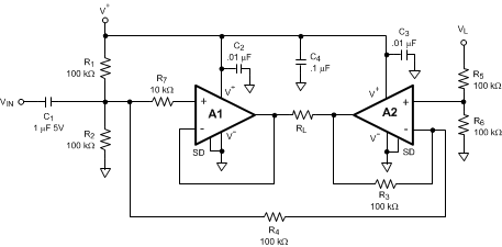
The circuit shown in Figure 50 can drive a long cable using only two wires; a combined single signal and power wire and ground. The robust output stage and low operating voltage of the LMV951 makes it an excellent choice for driving long cables.
 Figure 50. Two Wire Line Driver
8.2.1.1 Design Requirements
When many sensors are located remotely from the control area the wiring becomes a significant expense. Using only two wires helps minimize the wiring expense in a large project such as an industrial plant. It is desired to both provide a buffered signal from the sensor as well as provide power to the sensor amplifier.
8.2.1.2 Detailed Design Procedure
TI recommends a power supply of 3 V to power this system. A1 and A2 are set up as unity gain buffers. Configuring A1 with the required gain is simple if a gain of greater than one is required. C1 along with R1 and R2 are used to ensure the correct DC operating point at the input of A1.
C4 along with R5 and R6 are used to set up the correct DC operating point for A2. C1, C3, and C4 have been selected to give about a 20% droop with a 1-kHz square wave input.
8.2.2 Bridge Configuration Amplifier
 Figure 53. Bridge Amplifier
Some applications may benefit from doubling the voltage across the load. With V+ = 1 V a bridge configuration can provide a 2-VPP output to the load with a resistance as low as 300 Ω. The output stage of the LMV951 enables it to drive a load of 120 Ω and still swing at least 70% of the supply rails.
The bridge configuration shown in Figure 53 enables the amplifier to maintain a low dropout voltage thus maximizing its dynamic range. It has been configured in a gain of 1 and uses the fewest number of parts.
Resistor values have been selected to keep the current consumption to a minimum and voltage errors due to bias currents negligible. Using the selected resistor values makes this circuit quite practical in a battery operated design. R1, R2 and R5, R6 set up a virtual ground that is half of V+. The accuracy of the resistor values will establish how well the two virtual grounds match. Any errors in the virtual grounds will show as current across RL when there is no input signal.
AC coupling the input signal sets the DC bias point of this signal to the virtual ground of the circuit. Using the large resistor values with a 1-µF capacitor (C1) sets the frequency rolloff of this circuit below 10 Hz.
- C2 and C3 are .01-μF ceramic capacitors that must be located as close as possible to pin 6, the V+ pin. As covered in the power supply bypassing section these capacitors must have low ESR and a self resonant frequency above 15 MHz.
- C4 is a 1 μF tantalum or electrolytic capacitor that should also be located close to the supply pin.
- To use the shutdown feature tie pin 5 of the two parts together and connect through a 470-kΩ resistor to V+. Add a switch between pin 5 and ground. Closing the switch keeps the parts in the active mode, opening the switch sets the parts in the shutdown mode without adding any additional current to V+.
8.2.3 Virtual Ground Circuit
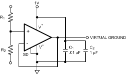
 Figure 54. Virtual Ground Circuit
Figure 54 shows the LMV951 being used in a system establishing a virtual ground. Having a buffered output stage gives this part the ability to handle load currents higher than 35 mA at 1 V.
R3 and R4 are used to set the voltage of the virtual ground. To maintain low noise the values should be from 1 kΩ to 10 kΩ. C1 and C2 provide the recommended bypassing for the LMV951. These capacitors must be placed as close as possible to pins 2 and 6.

