SNOSAI3D October 2006 – September 2015 LMV951
PRODUCTION DATA.
7 Detailed Description
7.1 Overview
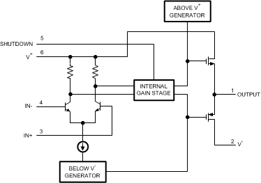
The LMV951 device is low-voltage operational amplifier that utilizes an internal charge pump which allows for full rail-to-rail input and output operation from 1-V to 3-V supplies. An internal switching frequency from 10 MHz to
15 MHz is used for generating the internal voltages.
7.2 Functional Block Diagram

7.3 Feature Description
7.3.1 Battery Operated Systems
The maximum operating voltage is 3 V and the operating characteristics are ensured down to 1 V which makes the LMV951 an excellent choice for battery operated systems using one or two NiCd or NiMH cells. The LMV951 is also functional at 0.9 V making it an appropriate choice for a single cell alkaline battery.
7.3.2 Small Size
The small footprint of the LMV951 package is ideal for high density board systems. By using the small 6-pin SOT package, the amplifier can be placed closer to the signal source, reducing noise pickup and increasing signal integrity.
7.4 Device Functional Modes
7.4.1 Shutdown Capability
While in shutdown mode, the LMV951 typically consumes less than 50 nA of supply current making it ideal for power conscious applications. Full functionality is restored within 3 μs of enable.
The output is in a high impedance state during shutdown. Voltages may be applied to the inputs and output during shutdown provided they are within the legal V+ to V- range.
7.4.2 Rail-to-Rail Input
The bipolar input stage provides rail-to-rail input operation with no input bias current reversal and a constant input offset voltage over the entire input common-mode range.
The input contains protection diodes between the inputs to limit the differential voltage (voltage between the input pins). The LMV951 should NOT be used for comparator applications as the diodes will clamp the inputs together. These diodes may also cause issues with follower configurations during shutdown as crosstalk may occur between the input pins through these diodes.
7.4.3 Rail-to-Rail Output
The CMOS output stage provides a gain that is virtually independent of resistive loads and an output drive current in excess of 35 mA at 1 V. A further benefit of the output stage is that the LMV951 is stable in positive unity gain at capacitive loads in excess of 1000 pF.
The internal charge pumps are used to provide the needed headroom for the internal gate drive circuitry and does not enable the output to swing beyond the rails. The output swing is still bound by the V+ and V- rails.
7.4.4 Driving Capacitive Load
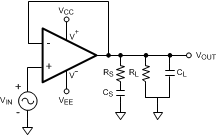
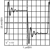
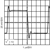
The unity gain follower is the most sensitive op amp configuration to capacitive loading. The LMV951 can drive up to 10,000 pF in this configuration without oscillation. If the application requires a phase margin greater than those shown in the datasheet graphs, a snubber network is recommended. The snubber offers the advantage of reducing the output signal ringing while maintaining the output swing which ensures a wider dynamic range; this is especially important at lower supply voltages.
 Figure 47. Snubber Network to Improve Phase Margin
Table 1 gives recommended values for some common values of large capacitors. For these values RL = 2 kΩ.
Table 1. Recommended Values for Snubbing Network
| CL | RS | CS |
|---|---|---|
| 500 pF | 330Ω | 6800 pF |
| 680 pF | 270Ω | 8200 pF |
| 1000 pF | 220Ω | .015 μF |
 Figure 48. 1000 pF and No Snubber
 Figure 49. 1000 pF With Snubber