JAJSG01D June 2012 – August 2018 LMZ20502
PRODUCTION DATA.
- 1 特長
- 2 アプリケーション
- 3 概要
- 4 改訂履歴
- 5 Pin Configuration and Functions
- 6 Specifications
- 7 Detailed Description
- 8 Application and Implementation
- 9 Power Supply Recommendations
- 10Layout
- 11デバイスおよびドキュメントのサポート
- 12メカニカル、パッケージ、および注文情報
パッケージ・オプション
デバイスごとのパッケージ図は、PDF版データシートをご参照ください。
メカニカル・データ(パッケージ|ピン)
- SIL|8
サーマルパッド・メカニカル・データ
発注情報
7.3.3 Current Limit Protection
The LMZ20502 incorporates cycle-by-cycle peak current limit on both the high and low side MOSFETs. This feature limits the output current in case the output is overloaded. During the overload, the peak inductor current is limited to that value found in the Electrical Characteristics table under the heading of "ILIM".
In addition to current limit, a short circuit protection mode is also implemented. When the feedback voltage is brought down to less than 300 mV, but greater than 150 mV, by a short circuit, the synchronous rectifier is turned off. This provides more voltage across the inductor to help maintain the required volt-second balance. If a "harder" short brings the feedback voltage to below 150 mV, the current limit and switching frequency are both reduced to about ½ of the nominal values. In addition, when the current limit is tripped, the device stops switching for about 85 µs. At the end of the time-out, switching resumes and the cycle repeats until the short is removed.
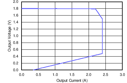
The effect of both overload and short circuit protection can be seen in Figure 9. This graph demonstrates that the device will supply slightly more than 2 A to the load when in overload and much less current during fold-back mode. This is typical behavior for any regulator with this type of current limit protection.
 Figure 9. Typical Current Limit Profile
VIN = 5 V, VOUT = 1.8 V