JAJSF83E June 2013 – February 2020 LMZ31707
PRODUCTION DATA.
- 1 特長
- 2 アプリケーション
- 3 概要
- 4 改訂履歴
- 5 Specifications
- 6 Device Information
- 7 Typical Characteristics (PVIN = VIN = 12 V)
- 8 Typical Characteristics (PVIN = VIN = 5 V)
- 9 Typical Characteristics (PVIN = 3.3 V, VIN = 5 V)
-
10Application Information
- 10.1 Adjusting the Output Voltage
- 10.2 Capacitor Recommendations for the LMZ31707 Power Supply
- 10.3 Transient Response
- 10.4 Transient Waveforms
- 10.5 Application Schematics
- 10.6 Custom Design With WEBENCH® Tools
- 10.7 VIN and PVIN Input Voltage
- 10.8 3.3 V PVIN Operation
- 10.9 Power Good (PWRGD)
- 10.10 SYNC_OUT
- 10.11 Parallel Operation
- 10.12 Light Load Efficiency (LLE)
- 10.13 Power-Up Characteristics
- 10.14 Pre-Biased Start-up
- 10.15 Remote Sense
- 10.16 Thermal Shutdown
- 10.17 Output On/Off Inhibit (INH)
- 10.18 Slow Start (SS/TR)
- 10.19 Overcurrent Protection
- 10.20 Synchronization (CLK)
- 10.21 Sequencing (SS/TR)
- 10.22 Programmable Undervoltage Lockout (UVLO)
- 10.23 Layout Considerations
- 10.24 EMI
- 11デバイスおよびドキュメントのサポート
- 12メカニカル、パッケージ、および注文情報
7 Typical Characteristics (PVIN = VIN = 12 V)
The electrical characteristic data has been developed from actual products tested at 25°C. This data is considered typical for the converter. Applies to Figure 1, Figure 2, and Figure 3. The temperature derating curves represent the conditions at which internal components are at or below the manufacturer's maximum operating temperatures. Derating limits apply to devices soldered directly to a 100-mm × 100-mm, 4-layer PCB with 2-oz. copper. Applies to Figure 4.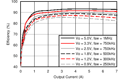 Figure 1. Efficiency versus Output Current
 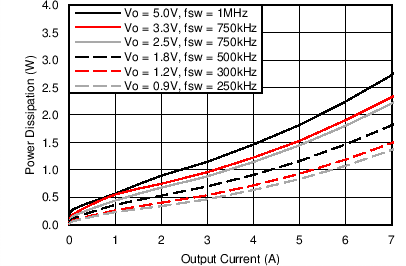 Figure 3. Power Dissipation versus Output Current
 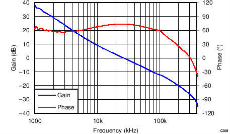 Figure 5. VOUT = 1.8 V, IOUT = 7 A, COUT = 200 µF Ceramic, fSW = 500 kHz
 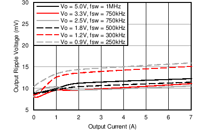 Figure 2. Voltage Ripple versus Output Current
 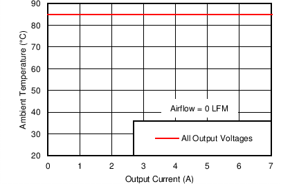 Figure 4. Safe Operating Area